MCU Interfaces

IRLZ44N Logic-Level N-Channel MOSFET Low-Side DC Switch

Discrete 12V/24V low-side DC switch circuit driving high-current inductive and resistive loads with an Infineon IRLZ44NPbF logic-level MOSFET from 3.3V or 5V MCU logic.

Load Supply Voltage (VLOAD)
+12.0 V DC nominal (+5.0 V to +50.0 V operating range)
Components
7
Formulas
4
Gotchas
4
Open in Web CAD
Verified source

Schematic workbench

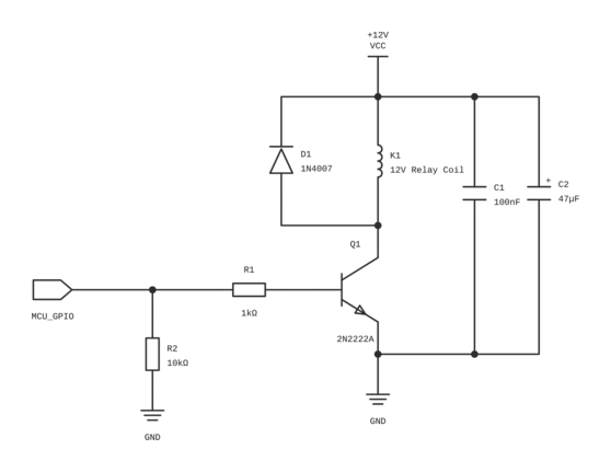
IRLZ44N Logic-Level N-Channel MOSFET Low-Side DC SwitchExported from CircuitBaseMCU_GPIOR1100ΩR210kΩGNDQ1IRLZ44NPbFD11N4007MM112V DC Motor+C1100µFC2100nFVCC+12VGND

Circuit overview

Load Supply Voltage (VLOAD)
+12.0 V DC nominal (+5.0 V to +50.0 V operating range)
Components
7
Formulas
4
Gotchas
4

Click any component in the schematic above to inspect its electrical ratings, function, and connections.

Circuit overview

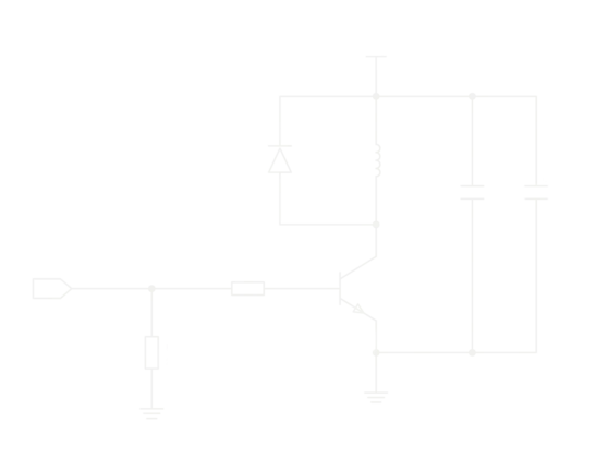
This discrete low-side DC power switch interfaces a 3.3V or 5.0V microcontroller GPIO directly with high-current DC loads operating from a +12V DC power rail (scalable up to +50V DC). The circuit utilizes the Infineon Technologies IRLZ44NPbF N-channel logic-level HEXFET power MOSFET in a through-hole TO-220AB package. The MOSFET source is connected directly to system power ground (GND), while the drain pulls down the low side of the load (LOAD-). To ensure dependable operation and protect the driving microcontroller, a series gate damping resistor R1 (100 Ω 1%) dampens parasitic LC ringing between PCB trace inductance and the transistor input capacitance (Ciss = 1700 pF), while bounding transient gate charging current to under 33 mA at 3.3V and 50 mA at 5.0V. A gate pull-down resistor R2 (10 kΩ 1%) holds the gate solidly at 0V during microcontroller power-up, firmware reboot, or ISP flashing when GPIO pins float in a high-impedance tri-state condition. For inductive loads (such as DC motors, solenoids, relays, or electromagnetic valves), a fast flyback clamp diode D1 (1N4007) is placed directly across the load terminals in reverse polarity, safely recirculating inductive collapse current and clamping the drain voltage to +12V + VF (approx. 13.0V), safely below the MOSFET 55V drain-source breakdown rating (V(BR)DSS). Power supply integrity is preserved by parallel bulk electrolytic decoupling C1 (100 µF 50V) and ceramic high-frequency bypass C2 (100 nF 50V), suppressing supply droop and inductive kickback across the DC bus.

Key Technical Specifications

Load Supply Voltage (VLOAD)+12.0 V DC nominal (+5.0 V to +50.0 V operating range)
Logic Control Voltage (VIN)+3.3 V to +5.0 V CMOS / TTL microcontroller logic
Continuous Drain Current (ID)Up to 10 A continuous (chassis heatsink required above 4 A)
MOSFET On-Resistance (RDS(on))≤ 25 mΩ at VGS = 5.0 V, ≤ 35 mΩ at VGS = 4.0 V (Infineon IRLZ44NPbF)
Gate Threshold Voltage (VGS(th))1.0 V minimum to 2.0 V maximum (ID = 250 µA, VDS = VGS)
Series Gate Resistor (R1)100 Ω 1% metal film (limits MCU inrush current and damps ringing)
Gate Pull-Down Resistor (R2)10 kΩ 1% metal film (guarantees OFF state during MCU boot/reset)
Flyback Clamp Diode (D1)1N4007 (1000 V, 1.0 A continuous, 30 A surge rating)
Power Decoupling (C1, C2)100 µF 50V electrolytic + 100 nF 50V X7R ceramic MLCC

Theory of Operation & Working Principle

01

Circuit Topology and Low-Side Switching Architecture

The circuit is organized as an N-channel low-side power switch. The load (M1, representing a brushed DC motor, solenoid, or high-power LED array) connects between the positive DC supply rail (+12 V nominal) and the drain terminal of the N-channel MOSFET Q1 (Infineon IRLZ44NPbF). The source terminal of Q1 connects directly to system ground (GND). Because the source voltage is permanently referenced to 0 V, the gate-to-source drive voltage (VGS) is identical to the gate terminal voltage (VG), allowing direct drive from single-ended microcontroller logic outputs without requiring bootstrap floating gate drivers or high-side charge pumps.
02

Phase 1: Default OFF State and Tri-State Reset Protection

When the microcontroller GPIO is at logic LOW (0 V) or unpowered, pull-down resistor R2 (10 kΩ) ties the gate to ground. Because VGS = 0 V, which is well below the gate threshold voltage range (VGS(th) = 1.0\dots 2.0 V), the inversion channel is completely closed. Drain cutoff leakage current is negligible (IDSS ≤ 25\ µA at 25°C), holding the load completely de-energized. During microcontroller bootloader execution, firmware reset, or ISP programming, GPIO pins default to high-impedance input mode; R2 prevents electrostatic charges or capacitive Miller coupling (Cgd) from unintentionally charging the gate into partial conduction.

03

Phase 2: Logic Turn-On Transition and Gate Charge Dynamics

When the microcontroller drives the GPIO pin HIGH (+3.3 V or +5.0 V), current flows through series damping resistor R1 (100 Ω) to charge the input capacitance (Ciss = 1700 pF, total gate charge Qg = 48 nC max at VGS = 5 V). Series resistor R1 limits the peak inrush current extracted from the microcontroller I/O pin (Ipeak ≤ 33 mA at 3.3 V, 50 mA at 5.0 V), preventing latch-up and internal output driver damage. As the gate voltage crosses the threshold voltage and traverses the flat Miller plateau (VGP ≈ 2.5\dots 3.0 V), the drain-to-source voltage abruptly collapses to near ground, establishing full channel conduction.

04

Phase 3: Saturated On-State Conduction and Low Dissipation

With a 5.0 V gate drive, the IRLZ44NPbF achieves a guaranteed on-resistance of RDS(on) ≤ 25 mΩ at ID = 25 A (TJ = 25°C). Even with a 3.3 V gate drive, the channel achieves an on-resistance under 35\dots 40 mΩ for moderate currents (ID ≤ 10 A). For a continuous load current of ILOAD = 5.0 A, the static conduction drop across the transistor is only VDS = ID · RDS(on) = 5.0 A × 0.025\ Ω = 0.125 V, resulting in continuous power dissipation of Pcond = ID2 · RDS(on) = (5.0 A)2 × 0.025\ Ω = 0.625 W. This low dissipation allows continuous operation with minimal heatsinking.

05

Phase 4: Inductive Turn-Off Dynamics and Flyback Diode Clamping

Design Equations & Calculations

Static Conduction Power Dissipation

Pcond = ID2 · RDS(on)

Calculates the continuous static thermal dissipation across the conducting MOSFET channel as a function of load current and gate-overdrive on-resistance.

SymbolParameterTypical value
PcondConduction Power Dissipation0.625W
IDContinuous Drain Current5.0A
RDS(on)Drain-Source On-State Resistance0.025Ω

Peak Transient Gate Charging Current

IG,peak = VINR1 + Rdrv

Determines the peak inrush current drawn from the microcontroller GPIO output during switching transitions to ensure safe operating limits.

SymbolParameterTypical value
IG,peakPeak Gate Charging Current33mA
VINMicrocontroller Logic High Voltage3.3V
R1Series Gate Damping Resistor100Ω
RdrvInternal GPIO Output Driver Resistance25Ω

Free-Air Junction Temperature Rise

TJ = TA + PD · θJA

Estimates steady-state silicon junction temperature in ambient free air without an external heatsink to evaluate thermal safety margins.

SymbolParameterTypical value
TJSilicon Junction Temperature63.75°C
TAAmbient Environmental Temperature25.0°C
PDTotal Transistor Power Dissipation0.625W
θJAJunction-to-Ambient Thermal Resistance62.0°C/W

Inductive Turn-Off Clamped Peak Voltage

VDS,peak = VLOAD + VF

Calculates the maximum peak drain voltage clamped by the freewheeling flyback diode during inductive load turn-off transients.

SymbolParameterTypical value
VDS,peakPeak Clamped Drain Voltage13.1V
VLOADLoad Supply Rail Voltage12.0V
VFFlyback Diode Forward Voltage Drop1.1V

Bill of Materials (BOM)

Every part needed to build this circuit. Select a reference designator to inspect it on the schematic.

RefDesComponentValue / ratingPackageRole in circuitReference
N-Channel Logic-Level Power MOSFET

Infineon Technologies 55V 47A logic-level HEXFET power MOSFET with RDS(on) <= 25 mΩ at VGS = 5V.

IRLZ44NPbFTO-220ABLow-Side High-Current Power SwitchN-Channel Logic-Level Power MOSFET pinout & datasheet
Gate Series Damping Resistor 100 Ω

100 Ω 1% 0.25W metal film resistor damping gate ringing and limiting peak MCU GPIO current.

100ΩAxial / 0805Parasitic Ringing Suppression & Inrush Limiting—
Gate Pull-Down Resistor 10 kΩ

10 kΩ 1% 0.25W metal film resistor holding gate at 0V during microcontroller boot and reset.

10kΩAxial / 0805Tri-State Reset & Float Protection—
Inductive Flyback Clamp Diode

1000V 1.0A standard recovery rectifier diode suppressing inductive turn-off voltage spikes.

1N4007DO-41Inductive Turn-Off Transient SuppressionInductive Flyback Clamp Diode pinout & datasheet
12V Brushed DC Motor

12V DC brushed motor load representing typical switched electromechanical inductive actuators.

12V DC MotorChassis MountSwitched Inductive Load—
Bulk Power Decoupling Electrolytic Capacitor 100 µF

100 µF 50V low-ESR radial electrolytic capacitor absorbing transient inductive load current spikes.

100µFRadial CAN 8x11.5mmDC Bus Voltage Stabilization—
High-Frequency Ceramic Bypass Capacitor 100 nF

100 nF 50V X7R ceramic capacitor bypassing high-frequency switching edges on DC power rail.

100nF0805 / RadialHigh-Frequency Noise Suppression—

Practical Applications & Target Domains

Driving high-current brushed DC motors, linear actuators, and cooling fans from ESP32, Arduino, or Raspberry Pi GPIO pins
Switching 12V and 24V industrial solenoids, electromagnetic valves, and latching mechanisms
High-power PWM dimming of 12V/24V constant-voltage LED lighting strips and architectural fixtures
Direct electronic control of automotive accessories, pumps, and resistive heating elements from low-voltage microcontrollers

Critical Design Traps & Engineering Gotchas

Traps found in real builds, with the fix for each.

Critical

Standard Vth MOSFET vs Logic-Level MOSFET Selection Trap (IRFZ44N vs IRLZ44N)

Substituting standard-threshold IRFZ44N in place of logic-level IRLZ44N. The IRFZ44N requires VGS = 10V to achieve low RDS(on); driven at 3.3V or 5V, it operates in the resistive linear region with high on-resistance, causing rapid thermal runaway and destruction under load.

Mitigation

Verify the part prefix: 'IRL' indicates logic-level gate drive with specified RDS(on) at 4V and 5V. For high currents at 3.3V logic, verify transfer characteristics or add a dedicated MOSFET gate driver buffer.

Critical

Floating Gate Voltage During Microcontroller Reset and Tri-State Boot

Omitting the 10 kΩ gate pull-down resistor leaves the high-impedance gate (>10^12 Ω) floating when MCU pins default to high-Z input mode during boot, reset, or flashing, allowing capacitive coupling to unintentionally energize the load.

Mitigation

Always install a 10 kΩ pull-down resistor directly between gate and source ground, placed physically close to the transistor terminals to minimize noise pickup.

Critical

Destructive Inductive Back-EMF Avalanche Without Flyback Diode

Switching inductive loads (motors, solenoids, relays) without an antiparallel freewheeling clamp diode forces inductive collapse energy into the MOSFET, driving drain voltage into avalanche breakdown above 55V and destroying the silicon.

Mitigation

Always install a fast catch diode (such as 1N4007 or Schottky 1N5819) directly across the inductive load terminals with cathode to +VLOAD and anode to Drain, sized for the full load operating current.

Warning

TO-220 Metal Mounting Tab Short-to-Ground Risk

The TO-220AB metal mounting tab is internally connected to Drain (Pin 2). In a low-side switch, the tab swings between 0V and +12V. Bolting the tab to a grounded metal chassis or common heatsink shorts the load return directly to ground, permanently energizing the load.

Mitigation

When mounting to a grounded heatsink or metal enclosure, always use an electrically insulating silicone or mica pad and an insulating shoulder washer around the mounting screw.

Primary sources

Help keep this page accurate

Built, simulated or reviewed this circuit? Confirm it, or report a part, value or connection that is wrong.

Opens a public form on GitHub with this page already filled in; a free GitHub account is needed. How reports and confirmations work

HTML snippet

<iframe src="https://circuitbase.tech/embed/schematic/irlz44n-logic-level-low-side-switch?theme=paper" width="100%" height="500" frameborder="0" loading="lazy" style="border: 1px solid #e5e7eb; border-radius: 6px; max-width: 100%;" title="IRLZ44N Logic-Level N-Channel MOSFET Low-Side DC Switch — CircuitBase Interactive Schematic"></iframe>