MCU Interfaces

2N2222 / 2N2222A NPN BJT Relay Driver with 1N4007 Flyback Clamping Diode

Discrete NPN bipolar junction transistor low-side relay driver circuit with 1N4007 flyback suppression diode, base saturation drive, and supply decoupling for 3.3V/5V MCU control.

Relay Supply Voltage (VLOAD)
+12.0 V DC nominal (+10.8 V to +13.2 V operating range)
Components
7
Formulas
4
Gotchas
4
Open in Web CAD
Verified source

Schematic workbench

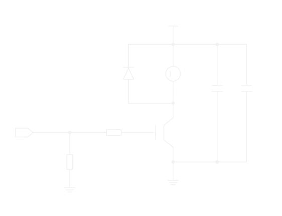
2N2222 NPN BJT Relay Driver with 1N4007 Flyback Clamping DiodeExported from CircuitBaseMCU_GPIOR11kΩR210kΩGNDQ12N2222AD11N4007K112V Relay CoilC1100nF+C247µFVCC+12VGND

Circuit overview

Relay Supply Voltage (VLOAD)
+12.0 V DC nominal (+10.8 V to +13.2 V operating range)
Components
7
Formulas
4
Gotchas
4

Click any component in the schematic above to inspect its electrical ratings, function, and connections.

Circuit overview

This classic discrete low-side driver interfaces standard 3.3V or 5.0V microcontroller GPIO outputs with a 12V electromechanical relay coil, providing galvanic isolation between logic circuits and high-voltage AC/DC loads. The switching core employs the industry-standard Central Semiconductor 2N2222A NPN bipolar junction transistor in a compact TO-92 through-hole package. The transistor operates strictly as a saturated electronic switch: when driven into saturation, the collector-emitter voltage collapses to VCE(sat) ≤ 0.3V, applying virtually the entire +12V power supply rail across the relay coil winding. Base drive is determined by series resistor R1 (1.0 kΩ 1%), which delivers 4.3 mA from 5.0V logic (or 2.6 mA from 3.3V logic). This establishes a forced current gain (forced beta) of βforced ≈ 7 to 15, well below the transistor minimum active gain (hFE(min) = 75 to 100), guaranteeing hard saturation across thermal variations and manufacturing tolerances. A base pull-down resistor R2 (10 kΩ 1%) holds the base solidly at 0V during microcontroller power-up, firmware reboot, or ISP flashing when GPIO pins float in high-impedance tri-state mode, preventing spurious coil energization and contact chatter. Crucially, a 1N4007 standard rectifier diode D1 is connected antiparallel across the coil terminals. Upon transistor turn-off, the rapid collapse of the coil magnetic field generates an inductive back-EMF transient (-L di/dt) that would otherwise exceed the 40V collector breakdown rating V(BR)CEO and destroy the transistor silicon; D1 clamps this transient to VCC + VF (approx. 13.1V), recirculating the inductive energy safely through the coil winding. Power supply bus stability is preserved by ceramic capacitor C1 (100 nF) and aluminum electrolytic capacitor C2 (47 µF), suppressing inductive switching noise and transient voltage dips.

Key Technical Specifications

Relay Supply Voltage (VLOAD)+12.0 V DC nominal (+10.8 V to +13.2 V operating range)
Logic Control Voltage (VIN)+3.3 V to +5.0 V CMOS / TTL microcontroller logic
Maximum Continuous Collector Current (IC)800 mA continuous (Central Semiconductor 2N2222A)
Collector-Emitter Breakdown Voltage (V(BR)CEO)40 V minimum
Saturation Voltage (VCE(sat))≤ 0.3 V at IC = 150 mA, IB = 15 mA (≤ 0.2 V typical at 30 mA)
Base Current-Limiting Resistor (R1)1.0 kΩ 1% metal film (sets IB = 4.25 mA at 5V, 2.55 mA at 3.3V)
Base Pull-Down Bleeder Resistor (R2)10 kΩ 1% metal film (guarantees cutoff during MCU boot/reset)
Flyback Clamping Diode (D1)1N4007 (1000 V VRRM, 1.0 A continuous, 30 A surge)
Relay Coil Nominal Current12.5 mA to 30.0 mA (Omron G5V-1-DC12 standard/high-sensitivity)
DC Rail Decoupling (C1, C2)100 nF 50V X7R ceramic MLCC + 47 µF 25V aluminum electrolytic

Theory of Operation & Working Principle

01

Circuit Topology and Low-Side Sinking Architecture

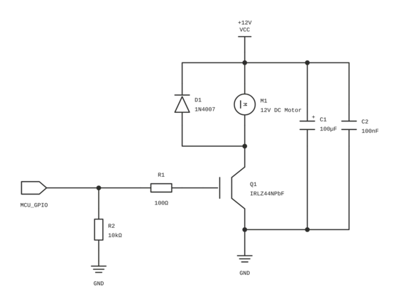
The circuit is organized as a common-emitter NPN low-side sink driver. The electromechanical relay coil (K1) connects between the positive DC power supply (+12 V nominal) and the collector terminal of transistor Q1 (Central Semiconductor 2N2222A). The emitter of Q1 connects directly to power ground (GND). When Q1 conducts, it completes the current path to ground, pulling the lower terminal of the relay coil down to VCE(sat) and energizing the coil winding. Because the emitter is fixed at 0 V, base-emitter drive voltage VBE is referenced directly to logic ground, enabling direct drive from single-ended microcontroller GPIO pins.
02

Phase 1: Microcontroller Boot Tri-State and Reset Clamping

When the driving microcontroller is powered off, held in reset, or executing early bootloader initialization, its GPIO pins reside in a high-impedance (tri-state) input mode. Pull-down bleeder resistor R2 (10 kΩ) ties the base terminal firmly to 0 V ground. This discharges any stray electrostatic charge or PCB leakage current (ICBO ≤ 10 nA), guaranteeing that VBE = 0 V. Because VBE remains far below the 0.65 V silicon PN junction conduction threshold, Q1 remains in cutoff mode (IC ≈ 0), completely de-energizing the relay coil and preventing false contact closures during boot.

03

Phase 2: Logic HIGH Transition and Base Saturation Drive

When the microcontroller drives the GPIO pin HIGH (+5.0 V from AVR/Arduino or +3.3 V from ESP32/STM32), forward bias is applied to the base-emitter junction. Base current IB is established across series limiting resistor R1:

FORMULA & CALCULATION
IB = (VIN - VBE(sat)) / (R1)

For a 5.0 V drive signal with VBE(sat) ≈ 0.75 V, base current is IB = (5.0 V - 0.75 V) / 1000\ Ω = 4.25 mA. For a typical 12V relay coil with Rcoil = 400\ Ω, nominal coil current is Icoil ≈ (12 V - 0.2 V) / 400\ Ω = 29.5 mA. The resulting forced current gain is:

FORMULA & CALCULATION
\betaforced = (IC) / (IB) = (29.5 mA) / (4.25 mA) ≈ 6.9

Because \betaforced \ll hFE(min) = 75, the transistor is pushed into deep hard saturation, causing excess minority carriers to flood the base region and driving collector-emitter voltage to its minimum saturation level (VCE(sat) ≤ 0.3 V).

04

Phase 3: Saturated Coil Energization and Thermal Dissipation

In saturation, the full power rail minus VCE(sat) appears across the relay coil (Vcoil ≈ 12.0 V - 0.2 V = 11.8 V). The magnetic field builds rapidly, pulling the armature inward and closing the normally-open (NO) mechanical contacts. Static conduction power dissipation in the transistor comprises collector and base components:

FORMULA & CALCULATION
PD = VCE(sat) × IC + VBE(sat) × IB
FORMULA & CALCULATION
PD = (0.2 V × 29.5 mA) + (0.75 V × 4.25 mA) = 5.9 mW + 3.2 mW = 9.1 mW

This negligible 9.1 mW dissipation is vastly below the 625 mW TO-92 thermal rating, maintaining the transistor at ambient room temperature without heatsinking.

05

Phase 4: Inductive Field Collapse and 1N4007 Flyback Clamping

When the microcontroller GPIO returns to logic LOW, base current drops to zero and Q1 transitions toward cutoff. The relay coil possesses significant magnetic inductance (L ≈ 0.5\dots 2 H). As current abruptly drops, the collapsing magnetic field induces a violent back-EMF voltage kick:

FORMULA & CALCULATION
vL = -L (di) / (dt)
FORMULA & CALCULATION
Vclamp = VCC + VF ≈ 12.0 V + 1.1 V = 13.1 V

The stored magnetic energy circulates harmlessly through the closed loop formed by D1 and the coil winding, dissipating as thermal energy in the coil resistance (Rcoil) until current decays to zero.

Design Equations & Calculations

Base Saturation Drive Current

IB = VIN − VBE(sat)R1

Calculates the base current delivered to the transistor in the active ON state to establish forced saturation overdrive.

SymbolParameterTypical value
IBBase Drive Current0.00425A
VINMicrocontroller GPIO Logic High Voltage5.0V
VBE(sat)Base-Emitter Saturation Voltage Drop0.75V
R1Base Series Resistor1000Ω

Forced Beta (Overdrive Ratio)

βforced = IcoilIB \ll hFE(min)

Evaluates the degree of saturation overdrive by comparing forced current gain against minimum datasheet active current gain.

SymbolParameterTypical value
βforcedForced Current Gain7.0ratio
IcoilRelay Coil Operating Current0.030A
IBBase Saturation Current0.00425A
hFE(min)Minimum Active DC Current Gain75ratio

Inductive Back-EMF Clamped Peak Voltage

Vclamp = VCC + VF(D1)

Determines the maximum peak voltage appearing at the transistor collector terminal during inductive coil turn-off field collapse.

SymbolParameterTypical value
VclampPeak Clamped Collector Voltage13.1V
VCCPositive Load Power Supply Voltage12.0V
VF(D1)Flyback Diode Forward Voltage Drop1.1V

Transistor Saturated Conduction Power Dissipation

PD = VCE(sat) · IC + VBE(sat) · IB

Calculates the total continuous electrical power dissipated as heat inside the transistor die during steady-state ON conduction.

SymbolParameterTypical value
PDTotal Transistor Power Dissipation0.0091W
VCE(sat)Collector-Emitter Saturation Voltage0.2V
ICCollector Current (Coil Current)0.030A
VBE(sat)Base-Emitter Saturation Voltage0.75V
IBBase Drive Current0.00425A

Bill of Materials (BOM)

Every part needed to build this circuit. Select a reference designator to inspect it on the schematic.

RefDesComponentValue / ratingPackageRole in circuitReference
NPN General Purpose Bipolar Transistor

Central Semiconductor 40V 800mA high-speed NPN transistor in TO-92 through-hole package.

2N2222ATO-92Low-Side Saturated Relay Driver SwitchNPN General Purpose Bipolar Transistor pinout & datasheet
General Purpose Rectifier / Clamp Diode

Micro Commercial Co 1000V 1.0A rectifier diode clamping turn-off back-EMF spikes across the coil.

1N4007DO-41Inductive Kickback Flyback SuppressionGeneral Purpose Rectifier / Clamp Diode pinout & datasheet
Subminiature SPDT Signal / Power Relay

Omron Electronics 12V DC coil subminiature SPDT relay with 960Ω coil and 1A 24VDC / 0.5A 125VAC contact rating.

G5V-1-DC12DIP-5 / THTGalvanically Isolated Electromechanical Actuator—
Base Current-Limiting Resistor 1 kΩ

1.0 kΩ 1% 0.25W metal film resistor establishing forced saturation base current from 3.3V/5V logic.

1kΩAxial / 0805Base Saturation Drive Limiter—
Base Pull-Down Bleeder Resistor 10 kΩ

10 kΩ 1% 0.25W metal film resistor clamping base to 0V ground during microcontroller reset.

10kΩAxial / 0805Tri-State Reset & Float Suppression—
High-Frequency Ceramic Decoupling MLCC

100 nF 50V X7R ceramic capacitor shunting inductive commutation noise directly at the supply bus.

100nF 50V0805 / RadialHigh-Frequency Noise Shunting—
Bulk Aluminum Electrolytic Decoupling

47 µF 25V low-ESR electrolytic capacitor absorbing pull-in current surges.

47µF 25VRadial CAN 6.3x11mmDC Bus Stabilization Reservoir—

Practical Applications & Target Domains

Interfacing Arduino, ESP32, STM32, and Raspberry Pi GPIO pins with 12V electromechanical relays
Driving pneumatic solenoid valves, electronic door strikes, and magnetic latching actuators
Galvanic mains AC switching (120V/240V lighting, heating elements, pump motors) via relay isolation
Automotive and industrial 12V auxiliary DC load switching with logic-level control signals

Critical Design Traps & Engineering Gotchas

Traps found in real builds, with the fix for each.

Critical

Destructive Inductive Back-EMF Avalanche Without Flyback Diode

Switching inductive relay coils without an antiparallel freewheeling diode forces magnetic collapse energy into the BJT. The collector voltage instantly spikes to hundreds of volts (-L di/dt), driving the transistor into avalanche breakdown above 40V and permanently puncturing the silicon junction.

Mitigation

Always install a dedicated flyback diode (such as 1N4007 or Schottky 1N5819) directly across the relay coil terminals with cathode to +12V and anode to collector, keeping loop trace length minimal to avoid parasitic inductance.

Critical

Insufficient Base Drive Current Leading to Linear Mode Operation

Selecting a base resistor that is too large (e.g., 10 kΩ or 47 kΩ) starves the transistor of base current. The transistor operates in its active linear region instead of hard saturation, causing VCE to remain at 2V to 6V, under-energizing the coil and causing rapid transistor overheating.

Mitigation

Design for a forced beta of βforced = IC / IB ≤ 10 to 15. For a 30 mA coil and 3.3V logic, use R1 = 1.0 kΩ, providing IB ≈ 2.5 mA and guaranteed hard saturation across all temperature conditions.

Critical

Floating Base Pin During Microcontroller Reset and Boot

Omitting base pull-down resistor R2 leaves the high-impedance base floating when MCU GPIO pins default to high-Z input mode during boot, reset, or in-circuit firmware programming. Ambient electromagnetic noise or finger proximity can trigger false relay clicking.

Mitigation

Always install a 10 kΩ pull-down resistor directly between base and ground, placed physically close to the transistor terminals to keep the base grounded until active firmware drive is asserted.

Warning

Relay Armature Release Delay Caused by Standard Silicon Diode

A standard flyback diode clamps coil collapse voltage to only +1.1V above VCC, causing coil current to decay slowly according to time constant τ = L / Rcoil. For high-speed applications, this prolongs mechanical contact opening time and causes contact arcing.

Mitigation

For standard DC relays, the 1N4007 is robust and reliable. When high-speed contact release (< 5 ms) is required, place a Zener diode (e.g. 24V) in series with the diode anode-to-anode, or use a parallel resistor-diode snubber to speed magnetic decay.

Primary sources

Help keep this page accurate

Built, simulated or reviewed this circuit? Confirm it, or report a part, value or connection that is wrong.

Opens a public form on GitHub with this page already filled in; a free GitHub account is needed. How reports and confirmations work

HTML snippet

<iframe src="https://circuitbase.tech/embed/schematic/2n2222-relay-driver-flyback-protection?theme=paper" width="100%" height="500" frameborder="0" loading="lazy" style="border: 1px solid #e5e7eb; border-radius: 6px; max-width: 100%;" title="2N2222 / 2N2222A NPN BJT Relay Driver with 1N4007 Flyback Clamping Diode — CircuitBase Interactive Schematic"></iframe>