Circuit Analysis
The ULN2003A 7-channel inductive load driver operates across five distinct electrical and magnetic stages:
1. **Logic Input Assertion & Darlington Base Conduction:** When the host controller drives an input port (e.g., P_IN1) HIGH (+5.0 V), current enters Pin 1 through the internal 2.7 kΩ series resistor. The voltage exceeds the dual base-emitter turn-on threshold (VBE1 + VBE2 ≈ 1.4 V), supplying ~1.3 mA of base current to the input transistor. The composite Darlington pair rapidly switches into active conduction.
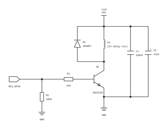
2. **Inductive Coil Energization & Low-Side Sinking:** The output transistor saturates, pulling Pin 16 (1C) down to VCE(sat) ≈ 1.1 V relative to ground (Pin 8). The relay coil L1 sees an effective differential voltage of VCC - VCE(sat) ≈ 12 V - 1.1 V = 10.9 V. Current builds exponentially according to i(t) = (V/R) * (1 - e^(-t / tau)), where tau = L / R, until full magnetic pull-in armature threshold is reached.
3. **Steady-State Saturation & Package Power Dissipation:** During continuous coil energization, current stabilizes at IC = (VCC - VCE(sat)) / R_coil. The Darlington pair dissipates electrical power PD = VCE(sat) * IC + VIN * IIN. With four channels energized at 150 mA each, total internal dissipation remains well within the 1.0 W thermal budget of the PDIP-16 package (junction-to-ambient thermal resistance R_thetaJA = 67 °C/W).
4. **Input Cut-Off & Inductive Field Collapse (Flyback Clamping):** When the input pin returns to logic LOW (0 V), base drive collapses. The Darlington pair switches OFF in under 0.5 µs. The sudden interruption of coil current causes an immediate inductive kickback (V_L = -L * dI/dt). The collector voltage flies above the +12 V supply rail until the internal clamp diode forward-biases at V_clamp = VCC + VF ≈ 12 V + 1.2 V = 13.2 V. The stored energy (E = 1/2 * L * I^2) circulates through the diode loop, safely converting into heat within the coil winding resistance.
5. **Supply Rail Decoupling & Ground Return Balancing:** As coils cycle on and off, switching transients generate localized dI/dt noise on the +12 V bus. Ceramic capacitor C1 (100 nF) shunts high-frequency spikes directly to ground, while electrolytic capacitor C2 (100 µF) provides local charge storage, preventing supply dips from resetting sensitive logic microcontrollers.