
01
Waiting state
Between pulses OUT (pin 3) is low and the discharge transistor on DISCH (pin 7) is on, holding C1 near 0 V. R2 keeps TRIG (pin 2) at VCC. RESET (pin 4) is tied to VCC, because a low RESET overrides everything else.
Timing & Oscillators
The one-shot circuit from the TI NE555 datasheet: press START and the output stays high for a fixed time set by one resistor and one capacitor, about 1.1 s with 100 kΩ and 10 µF.
Circuit overview
Click any component in the schematic above to inspect its electrical ratings, function, and connections.
This is Figure 6-2 of the Texas Instruments 555 timer datasheet (SLFS022K), the monostable or one-shot mode. A short low pulse on the trigger input starts a single output pulse whose length depends only on R1 and C1: tw = 1.1 × RA × C. Because the trigger and threshold levels are both fixed fractions of the supply, the pulse length does not change with the supply voltage as long as the supply stays constant during the pulse. TI draws a bare input line; here a START button with a 10 kΩ pull-up drives it, and the values RA = 100 kΩ and C = 10 µF give a pulse of about 1.1 s. A 10 nF capacitor on CONT and a 100 nF supply bypass complete the circuit, the latter as TI recommends in its power-supply section.
| Operating Supply Voltage | 4.5 V – 16 V (TI §7.3) |
|---|---|
| Pulse Length | tw = 1.1 × RA × C ≈ 1.1 s with 100 kΩ and 10 µF (calculated) |
| Trigger Level | 1/3 VCC; 1.67 V typical at VCC = 5 V (TI §5.5) |
| Threshold Level | 2/3 VCC; 3.3 V typical at VCC = 5 V (TI §5.5) |
| Supply Sensitivity of Timing | 0.1 %/V typical, 0.5 %/V maximum, monostable (TI §5.6) |
| Temperature Coefficient of Timing | 50 ppm/°C typical, monostable (TI §5.6) |
| Output Current | ±200 mA recommended (TI §5.3) |
Between pulses OUT (pin 3) is low and the discharge transistor on DISCH (pin 7) is on, holding C1 near 0 V. R2 keeps TRIG (pin 2) at VCC. RESET (pin 4) is tied to VCC, because a low RESET overrides everything else.
Pressing START pulls TRIG below the trigger level, one third of VCC (1.67 V typical at VCC = 5 V). The internal flip-flop sets: OUT goes high and the discharge transistor turns off, so C1 is free to charge.
C1 charges through R1 toward VCC:
VC(t) = VCC(1 - e^(-t/(RA C)))The pulse ends when V_C reaches the threshold of two thirds of VCC, which happens after ln 3 ≈ 1.1 time constants:
tw = RA C ln 3 ≈ 1.1 × RA C = 1.1 × 100 kΩ × 10\,µF = 1.1 sBoth levels scale with VCC, so the pulse length does not depend on the supply voltage while it stays constant. TI gives a supply sensitivity of 0.1 %/V typical for this mode.
At the threshold the flip-flop resets: OUT goes low and the discharge transistor turns on and empties C1, ready for the next trigger. TI notes that the sequence ends only if TRIG has been high for at least 10 µs before the end of the interval; if START is still held, OUT stays high until it is released.
OUT can source or sink up to 200 mA, enough for an LED with a series resistor, a small relay through a flyback diode, or a logic input.
Duration of the output pulse (TI §6.3.1).
| Symbol | Parameter | Typical value |
|---|---|---|
| RA | Timing resistor | 100kΩ |
| C | Timing capacitor | 10µF |
| tw | Pulse length (calculated) | 1.1s |
C1 charges toward VCC; the pulse ends when V_C reaches 2/3 VCC, at t = ln 3 · RA·C.
| Symbol | Parameter | Typical value |
|---|---|---|
| VCC | Supply voltage | 5V |
| RA C | Time constant | 1s |
Every part needed to build this circuit. Select a reference designator to inspect it on the schematic.
| RefDes | Component | Value / rating | Package | Role in circuit | Reference |
|---|---|---|---|---|---|
| Precision Timer TI NE555P; other 555 variants need their own supply and output checks. | NE555P | PDIP-8 | Monostable timer | Precision Timer pinout & datasheet | |
| Resistor | 100kΩ | Axial 1/4 W | Timing resistor RA | — | |
| Aluminium Electrolytic Capacitor Low-leakage type; + to THRES/DISCH; voltage rating above VCC. | 10µF | Radial | Timing capacitor | — | |
| Ceramic Capacitor | 10nF | 0805 / radial | CONT bypass | — | |
| Ceramic Capacitor Close to pins 8 and 1. | 100nF | 0805 / radial | Supply bypass | — | |
| Resistor | 10kΩ | Axial 1/4 W | Trigger pull-up | — | |
| Tactile Switch | START | SMD / THT | Trigger | — |
Traps found in real builds, with the fix for each.
The pulse ends only if TRIG has been high for at least 10 µs before the timing interval runs out. If START is held longer than tw, OUT stays high until it is released.
Keep the trigger shorter than the pulse. Where the input can stay low, couple it through a small capacitor so that only its falling edge reaches TRIG.
Near the threshold only (VCC − 2/3 VCC)/RA flows into C1, about 17 µA with 100 kΩ at 5 V (calculated). An electrolytic with high leakage takes a noticeable part of that current, lengthens the pulse, and with a very large RA may never reach the threshold.
Keep RA within the 2 kΩ – 100 kΩ range TI uses for its timing specifications and make the time longer with C, using a low-leakage capacitor; use film capacitors for short, accurate pulses.
CONT carries the internal threshold. Left open, noise coupled into it moves the threshold and makes the pulse length jitter.
Bypass CONT to ground with a small capacitor (10 nF here), as TI draws in Figure 6-2.
RESET is active low and overrides the trigger. Left floating it can pick up noise and end or block pulses.
Tie RESET to VCC as drawn, or drive it from logic if the pulse must be cancelled.
Built, simulated or reviewed this circuit? Confirm it, or report a part, value or connection that is wrong.
Opens a public form on GitHub with this page already filled in; a free GitHub account is needed. How reports and confirmations work
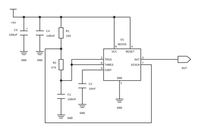
Standard astable relaxation oscillator topology outputting continuous square wave clock pulses with adjustable duty cycle.
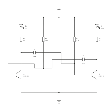

Discrete two-transistor cross-coupled relaxation oscillator driving alternating LEDs without an integrated circuit.
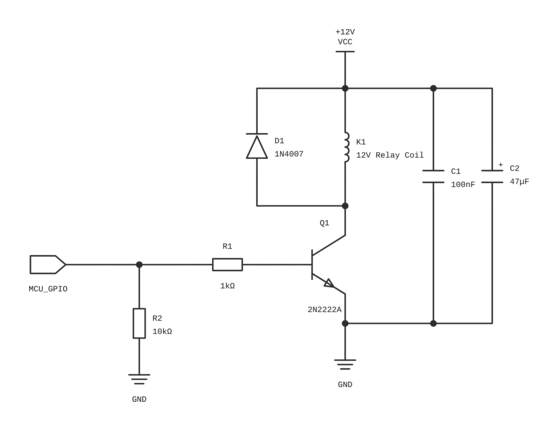
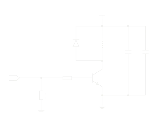
Discrete NPN bipolar junction transistor low-side relay driver circuit with 1N4007 flyback suppression diode, base saturation drive, and supply decoupling for 3.3V/5V MCU control.