Discrete two-transistor cross-coupled relaxation oscillator driving alternating LEDs without an integrated circuit.
Nominal Operating Supply Voltage
5.0 V DC nominal design assumption for educational demonstration. Requires sufficient headroom above the blue LED forward voltage (~3.3 V typ) to bias collector and base resistors; reverse base-emitter transients must remain within the transistor's absolute maximum rating (VEBO = 6.0 V for 2N3904BU).
5.0 V DC nominal design assumption for educational demonstration. Requires sufficient headroom above the blue LED forward voltage (~3.3 V typ) to bias collector and base resistors; reverse base-emitter transients must remain within the transistor's absolute maximum rating (VEBO = 6.0 V for 2N3904BU).
Components
10
Formulas
3
Gotchas
3
Click any component in the schematic above to inspect its electrical ratings, function, and connections.
Circuit overview
The BJT Astable Multivibrator is a classical discrete relaxation oscillator circuit. Two NPN bipolar junction transistors (Q1 and Q2) are configured in a cross-coupled feedback topology, where the collector of each transistor is AC-coupled to the base of the opposite transistor via timing capacitors C1 and C2. Under idealized symmetrical DC conditions, both transistors would theoretically be biased into simultaneous conduction; in practical hardware, minute component tolerances, device parameter variations, and ambient thermal noise can break this symmetry upon power application and initiate regenerative oscillation; startup is not guaranteed over component variation, supply ramps or temperature. Once oscillation is established, the circuit alternates between two quasi-stable states, generating complementary switching transitions that alternate the illumination of LED1 (D1) and LED2 (D2). Series collector resistors (R1 and R4) limit forward LED current, while base pull-up resistors (R2 and R3) supply sustained base bias from VCC and govern timing capacitor recharge rates.
Reference: T-multivibrator.svg by Д.Ильин (CC0 1.0). This fresh CircuitBase CAD adaptation adds series red/blue LEDs, selected nominal values and nonpolar MLCC timing capacitors to the basic two-transistor reference, which contains no LEDs or component values. The reference does not validate these added hardware choices or the calculated timing.
Key Technical Specifications
Nominal Operating Supply Voltage
5.0 V DC nominal design assumption for educational demonstration. Requires sufficient headroom above the blue LED forward voltage (~3.3 V typ) to bias collector and base resistors; reverse base-emitter transients must remain within the transistor's absolute maximum rating (VEBO = 6.0 V for 2N3904BU).
Oscillation Frequency (Ideal Reference Model)
≈1.54 Hz calculated ideal textbook estimate (f ≈ 1 / (1.386 · R · C) for R=47 kΩ, C=10 µF under simplified zero-offset assumptions). Physical frequency depends on LED forward drops, collector recharge time, and component tolerances, requiring transient simulation or bench measurement for exact figures.
Nominal Duty Cycle (Symmetrical Ideal Reference)
50% under ideal identical half-periods (T1 = T2 = ln(2) · R · C). Practical builds exhibit duty cycle divergence due to unequal LED forward voltages (Red ~1.9 V vs Blue ~3.3 V) and resistor/capacitor tolerances.
Transistor Type and Ratings
NPN Silicon Epitaxial Planar BJT (onsemi 2N3904BU, Case 135AN TO-92; absolute maximum ratings at TA=25°C: VCEO=40 V, IC=200 mA, VEBO=6.0 V; breakdown test V(BR)EBO ≥ 6.0 V at IE=10 µA, IC=0)
Timing Capacitors
C1 and C2: Murata GRM31CR71E106KA12L, nominal 10 µF ±10%, DC 25 V, X7R, EIA 1206. Effective capacitance in this timing circuit must be evaluated under actual voltage, AC amplitude, temperature and aging; 1.535 Hz remains a nominal ideal reference, not guaranteed physical timing.
Theory of Operation & Working Principle
01
Circuit Startup and Initial Cycle Inception
Upon DC power connection (VCC = 5.0 V nominal), timing capacitors C1 and C2 are initially uncharged. Base pull-up resistors R2 and R3 supply charging current from VCC to the bases of Q1 and Q2. In an ideal mathematical circuit with perfectly identical components and zero noise, both transistors would turn on equally toward a symmetrical equilibrium. In practical physical circuits, microscopic variations in base-emitter threshold voltage (VBE), current gain (hFE), and resistor tolerances, along with power supply rise times and ambient thermal noise, can break symmetry so that one transistor (e.g., Q1) conducts slightly more rapidly than the other. Regenerative feedback immediately accelerates this unbalance: as Q1 conducts, its collector voltage falls, coupling a negative potential through C1 to the base of Q2, which can drive Q2 off and initiate oscillation. This narrative does not guarantee startup for every component selection, supply ramp or temperature.
02
Established Cycle State Transition (Q1 Turn-On, Q2 Cutoff)
The following is a pedagogical step model of established oscillation, not a measured waveform: assume fixed conducting-collector voltage, constant illustrative VBE and VCE(sat), negligible base loading, and the stated off-collector voltage. Actual off-collector voltage depends on LED current and capacitor recovery. The general instantaneous coupling relation is VB(after) = VB(before) + VC(after) − VC(before). Immediately before Q1 turns on, Q2 is conducting in saturation with VB2(0-) ≈ VBE(on) ≈ 0.7 V, and Q1 is cut off with its collector resting near (VCC - VF(D1)). When Q1 snaps into saturation, its collector voltage plunges rapidly to VCE(sat) ≈ 0.15 V - 0.2 V. Because the charge on timing capacitor C1 cannot change instantaneously, charge continuity dictates the resulting base voltage of Q2:
FORMULA & CALCULATION
VB2(0^+) ≈ VBE(on) - ((VCC - VF(D1)) - VCE(sat))
In an illustrative simplified step calculation with assumed parameters (the LED datasheet VF at its stated test current is not a measured drop in this circuit) (VCC = 5.0 V, Red LED VF(D1) ≈ 1.9 V, VCE(sat) ≈ 0.2 V, VBE(on) ≈ 0.7 V), the collector voltage step is ΔVC ≈ 2.9 V, which couples across C1 to drive VB2(0+) negative to approximately -2.2 V. This reverse-biases the base-emitter junction of Q2, driving it firmly into cutoff and extinguishing Blue LED D2, while Q1 conducts and illuminates Red LED D1.
03
Quasi-Stable Timing Interval 1 (Q1 ON, Q2 OFF)
While Q2 remains cut off, its collector node is pulled toward VCC through R4 and D2, restoring charge onto the collector plate of C2. Sustained DC base current to keep Q1 saturated is supplied directly from VCC through pull-up resistor R2 (IB1 ≈ (VCC - VBE(on)) / R2). Simultaneously, timing capacitor C1 (whose negative side is connected to Q2's base) discharges its negative potential and recharges toward +VCC through base pull-up resistor R3 (47 kΩ). In this simplified model with a fixed opposite capacitor terminal and negligible transistor input current, the base voltage follows:
FORMULA & CALCULATION
VB2(t) = VCC - (VCC - VB2(0^+)) e^(-t / (R3 C1))
Transistor Q2 remains in cutoff throughout the interval until VB2(t) reaches the forward conduction threshold VBE(on) ≈ 0.65 V - 0.70 V. Solving for VB2(T1) = VBE(on) yields the cutoff duration:
When VB2(t) reaches VBE(on), transistor Q2 begins conducting base current. Regenerative cross-coupling rapidly pulls Q2 into saturation. As Q2's collector drops from (VCC - VF(D2)) down to VCE(sat) ≈ 0.2 V, this negative voltage step is coupled through timing capacitor C2 to the base of Q1:
FORMULA & CALCULATION
VB1(0^+) ≈ VBE(on) - ((VCC - VF(D2)) - VCE(sat))
For Blue LED D2 (illustrative VF(D2) ≈ 3.3 V), the collector voltage step ΔVC ≈ (5.0 - 3.3) - 0.2 = 1.5 V drives VB1(0+) down to approximately 0.7 V - 1.5 V = -0.8 V, cutting off Q1 and extinguishing Red LED D1, while Q2 conducts and illuminates Blue LED D2.
05
Quasi-Stable Timing Interval 2 and Timing Approximations
Transistor Q1 is held in cutoff while C2 recharges toward +VCC through base resistor R2 (47 kΩ). Sustained base current for Q2 is supplied from VCC through R3. The base voltage VB1(t) rises exponentially until reaching VBE(on), snapping Q1 back on and restarting the cycle.
In standard idealized textbook analysis, diode forward drops and transistor saturation offsets are neglected (VB(0+) ≈ -VCC, VBE(on) ≈ 0). Under these ideal reference assumptions, the half-period equations simplify to:
For symmetrical components (R2 = R3 = 47 kΩ, C1 = C2 = 10µF), this ideal textbook reference yields T ≈ 1.386 · R · C ≈ 0.651 s (f ≈ 1.535 Hz) with 50% duty cycle. In physical circuits, unequal forward LED drops (VF(D1) ≠ VF(D2)), finite collector pull-up recovery via RC, and component tolerances alter the switching thresholds and restore intervals. Accurate prediction of physical waveform timing requires full transient simulation or laboratory oscilloscope measurement.
Design Equations & Calculations
Ideal Reference Half-Period (Q2 Cutoff)
T1 = ln(2) · R3 · C1 ≈ 0.693 · R3 · C1
Calculates the ideal textbook cutoff duration in seconds for Transistor Q2 (while Q1 conducts and LED1 illuminates) as capacitor C1 recharges through base pull-up resistor R3 toward VCC, assuming zero forward diode drops and negligible transistor saturation voltages.
Symbol
Parameter
Typical value
R3
Base Pull-Up Resistor for Q2
47kΩ
C1
Timing Capacitor 1
10µF
Total Oscillation Period and Frequency (Ideal Reference)
Total ideal relaxation oscillation frequency in Hertz under simplified textbook assumptions. For symmetrical networks (R2=R3=R, C1=C2=C), simplifies to f ≈ 1 / (1.386 · R · C) ≈ 1.535 Hz. In physical hardware, forward LED drops, finite collector pull-up recovery, and component tolerances alter the effective charging bounds, requiring transient simulation or laboratory measurement for exact timing.
Symbol
Parameter
Typical value
T1
Half-Period 1 (Ideal Calculation Benchmark)
0.326s
T2
Half-Period 2 (Ideal Calculation Benchmark)
0.326s
R2
Q1 Base Resistor (Ideal Calculation Benchmark)
47kΩ
R3
Q2 Base Resistor (Ideal Calculation Benchmark)
47kΩ
C1
Timing Capacitor 1 (Ideal Calculation Benchmark)
10µF
C2
Timing Capacitor 2 (Ideal Calculation Benchmark)
10µF
LED Branch Current Estimate
ILED ≈ VCC − VF − VCE(sat)RC
Quasi-steady Ohmic approximation for the LED/resistor branch using actual LED forward voltage and an assumed conducting-collector voltage. It excludes coupling-capacitor transients and is not the total transistor collector current during switching.
Symbol
Parameter
Typical value
VCC
Supply Voltage
5.0V
VF
LED Forward Voltage Drop (Illustrative Calculation Value)
2.0V
VCE(sat)
Transistor Saturation Voltage (Illustrative Assumption)
0.2V
RC
Collector Limiting Resistor (R1 or R4)
1kΩ
Bill of Materials (BOM)
Every part needed to build this circuit. Select a reference designator to inspect it on the schematic.
RefDes
Component
Value / rating
Package
Role in circuit
Reference
NPN Bipolar Junction Transistor
onsemi 2N3904BU through-hole BJT (Rev. 3, Oct 2024, order code BU, Case 135AN); absolute maximum ratings at TA=25°C: VCEO=40V, IC=200mA, VEBO=6.0V; breakdown V(BR)EBO ≥ 6.0V (tested at IE=10µA, IC=0)
2N3904BU
TO-92 (Case 135AN)
Primary cross-coupled switching transistor
—
NPN Bipolar Junction Transistor
onsemi 2N3904BU through-hole BJT (Rev. 3, Oct 2024, order code BU, Case 135AN); absolute maximum ratings at TA=25°C: VCEO=40V, IC=200mA, VEBO=6.0V; breakdown V(BR)EBO ≥ 6.0V (tested at IE=10µA, IC=0)
2N3904BU
TO-92 (Case 135AN)
Complementary cross-coupled switching transistor
—
Carbon Film Resistor 1/4W
Yageo CFR-25JB-52-1K, 1.0 kΩ ±5%, 0.25 W at TA=70°C, carbon film; derate above 70°C
1kΩ
Axial Leaded
LED1 collector current limiting resistor
—
Carbon Film Resistor 1/4W
Yageo CFR-25JB-52-47K, 47 kΩ ±5%, 0.25 W at TA=70°C, carbon film; derate above 70°C
47kΩ
Axial Leaded
Base pull-up timing resistor for Q1 (governs T2 with C2)
—
Carbon Film Resistor 1/4W
Yageo CFR-25JB-52-47K, 47 kΩ ±5%, 0.25 W at TA=70°C, carbon film; derate above 70°C
47kΩ
Axial Leaded
Base pull-up timing resistor for Q2 (governs T1 with C1)
—
Carbon Film Resistor 1/4W
Yageo CFR-25JB-52-1K, 1.0 kΩ ±5%, 0.25 W at TA=70°C, carbon film; derate above 70°C
1kΩ
Axial Leaded
LED2 collector current limiting resistor
—
Nonpolar X7R Multilayer Ceramic Capacitor
Murata GRM31CR71E106KA12L, nominal 10 µF ±10%, rated DC 25 V, X7R, EIA 1206 (3216M); 01CA specification Jun. 25, 2026. Nominal capacitance is measured at room temperature, 1.0 ±0.1 kHz and 1.0 ±0.2 Vrms; effective capacitance depends on actual bias, AC amplitude, temperature and aging. No component-catalog lifecycle or application validation is implied.
10µF
EIA 1206 (3216M)
Timing capacitor coupling Q1 collector to Q2 base
—
Nonpolar X7R Multilayer Ceramic Capacitor
Murata GRM31CR71E106KA12L, nominal 10 µF ±10%, rated DC 25 V, X7R, EIA 1206 (3216M); 01CA specification Jun. 25, 2026. Nominal capacitance is measured at room temperature, 1.0 ±0.1 kHz and 1.0 ±0.2 Vrms; effective capacitance depends on actual bias, AC amplitude, temperature and aging. No component-catalog lifecycle or application validation is implied.
10µF
EIA 1206 (3216M)
Timing capacitor coupling Q2 collector to Q1 base
—
Standard 5mm Red Indicator LED
Kingbright WP7113ID, standard 5mm red LED (dominant 617nm, peak 627nm), VF = 1.9V typ (2.3V max) at IF = 10mA, TA = 25°C; absolute maximum continuous IF = 30mA at TA=25°C; datasheet VF footnote: ±0.1 V. These are specified test-point values, not guaranteed voltage or current in this circuit.
Red
T-1 3/4 (5mm)
Visual state indicator for channel 1 (active when Q1 conducts)
—
Standard 5mm Blue Indicator LED
Kingbright WP7113QBC/D, standard 5mm blue LED (dominant 465nm, peak 460nm), VF = 3.3V typ (4.0V max) at IF = 20mA, TA = 25°C; absolute maximum continuous IF = 30mA at TA=25°C; datasheet VF footnote: ±0.1 V. These are specified test-point values, not guaranteed voltage or current in this circuit.
Blue
T-1 3/4 (5mm)
Visual state indicator for channel 2 (active when Q2 conducts)
—
Practical Applications & Target Domains
✓Visual warning beacons and dual-LED alternating signal blinkers
✓Educational electronics laboratory demonstrations of regenerative switching and BJT relaxation oscillation
✓Basic cross-coupled discrete timing oscillator study
Critical Design Traps & Engineering Gotchas
Traps found in real builds, with the fix for each.
Critical
Reverse Base-Emitter Voltage Stress (Vebo = 6.0V Rating Limit)
When either switching transistor turns on, the negative voltage step at its collector couples across the timing capacitor to the opposite base node. The onsemi 2N3904BU datasheet specifies an absolute maximum emitter-base voltage rating of VEBO = 6.0 V (with breakdown test V(BR)EBO ≥ 6.0 V at IE = 10 µA, IC = 0). If an astable multivibrator is operated at higher supply voltages or with resistive collectors lacking series LED drops, the negative base excursion can exceed this VEBO rating. Repetitive reverse breakdown of the base-emitter junction can cause junction stress, potentially leading to cumulative degradation of transistor current gain (hFE) and elevated base leakage.
Mitigation
The illustrative step assumptions at nominal 5.0 V give reverse base excursions below the 6.0 V absolute limit; they are not a validated worst-case operating envelope. Check actual transients. A reverse clamp, if added, has anode at GND and cathode at the NPN base; such diodes are absent from this CAD and change timing, so reevaluate the circuit before using them.
Warning
Nonpolar Timing Capacitor Application Limits
Use a nonpolar timing capacitor because its terminal voltage reverses during the cycle. The selected Murata X7R MLCC has a 25 V DC rating, but capacitance tolerance and voltage/temperature/aging dependence can change timing. Nonpolarity does not by itself establish repetitive-waveform suitability or lifetime. The nominal 5.0 V educational step model gives capacitor voltages of a few volts; this is not a validated worst-case waveform envelope.
Mitigation
For the exact 01CA specification, keep the greater of peak-to-peak and zero-to-peak applied voltage within 25 V when AC is superimposed on DC. For AC/pulse use, check actual current and body self-heating: below 20°C rise at 25°C ambient for this <100 V DC-rated part, and total surface temperature at or below 125°C. Assess actual capacitance in the timing circuit and verify waveform and heating before claiming application readiness. No ripple-current, frequency, startup or lifetime guarantee is asserted.
Note
Metastable Equilibrium at Power-Up
Theoretical analysis indicates a possible symmetric equilibrium where both transistors conduct in forward active mode or saturation simultaneously with identical collector potentials. If the DC supply voltage rises very slowly or ramps monotonically in a heavily decoupled environment, both transistors may draw base current simultaneously through R2 and R3 without triggering regenerative oscillation.
Mitigation
In typical physical breadboard builds, inherent component variations (such as differences in hFE and VBE) and ambient thermal noise are usually sufficient to initiate oscillation upon rapid power connection. To avoid startup stall in production or slow-ramp environments, a dedicated timer IC (e.g. NE555) or an asymmetrical startup network should be utilized rather than relying on unassisted discrete BJT cross-coupling.
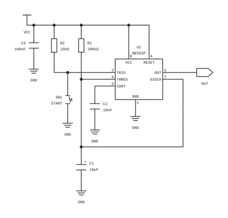
The one-shot circuit from the TI NE555 datasheet: press START and the output stays high for a fixed time set by one resistor and one capacitor, about 1.1 s with 100 kΩ and 10 µF.