
01
Timing & Oscillators
NE555 Astable Square Wave Generator
Standard astable relaxation oscillator topology outputting continuous square wave clock pulses with adjustable duty cycle.
- Operating Supply Voltage
- 4.5 V – 16 V DC (Texas Instruments NE555; shown circuit uses +5 V)
- Components
- 7
- Formulas
- 4
- Gotchas
- 2
Circuit overview
- Operating Supply Voltage
- 4.5 V – 16 V DC (Texas Instruments NE555; shown circuit uses +5 V)
- Components
- 7
- Formulas
- 4
- Gotchas
- 2
Click any component in the schematic above to inspect its electrical ratings, function, and connections.
Circuit overview
The NE555 timer in astable mode is a self-triggering relaxation oscillator based on two internal voltage comparators, an SR flip-flop, and an open-collector NPN discharge transistor. Operating entirely autonomously without external clock pulses, the circuit alternately charges and discharges timing capacitor C1 between 1/3 VCC and 2/3 VCC, producing a continuous digital square wave at Pin 3.
Key Technical Specifications
| Operating Supply Voltage | 4.5 V – 16 V DC (Texas Instruments NE555; shown circuit uses +5 V) |
|---|---|
| Maximum Output Drive Current | 200 mA (Sink / Source capability) |
| Nominal Design Frequency | 139 Hz (with R1 = 10 kΩ, R2 = 47 kΩ, C1 = 100 nF); calculated ideal value, not measured |
| Operating Frequency Range | Changing R1, R2 and C1 changes frequency; TI recommends NE555 operation at 100 kHz or below |
| Nominal Duty Cycle | 54.8% (Design values: R1 = 10 kΩ, R2 = 47 kΩ); calculated ideal value, not measured |
| Adjustable Duty Cycle Range | Ideal topology: greater than 50% and less than 100%; changing R1/R2 is required (no adjustment control fitted) |
| Timer Timing-Interval Temperature Coefficient | 150 ppm/°C typical in astable mode; excludes external resistor/capacitor drift (TI SLFS022K §5.6) |
Theory of Operation & Working Principle
02
Upper Threshold Crossing: When the voltage across C1 reaches 2/3 VCC, Pin 6 (THRESHOLD) triggers the internal upper comparator. This resets the flip-flop: Pin 3 snaps LOW (near GND), and the internal discharge transistor turns ON, clamping Pin 7 to ground.
03
Discharging Phase (Output LOW): With Pin 7 pulled to ground by the internal open-collector NPN transistor, current from VCC through R1 shunts directly to ground, while timing capacitor C1 discharges strictly through resistor R2 into Pin 7 with time constant tau_discharge = R2 * C1. Voltage on C1 decays exponentially toward ground.
04
Cycle Repetition: When C1 voltage falls below 1/3 VCC, Pin 2 (TRIGGER) detects the low voltage, setting the flip-flop again: Pin 3 goes HIGH, Pin 7 turns OFF, and C1 recharges. This cycle repeats continuously.
Design Equations & Calculations
High Time (Output HIGH)
thigh = ln(2) · (R1 + R2) · C1 ≈ 0.693 · (R1 + R2) · C1
Calculates the duration in seconds that output Pin 3 stays at logic HIGH while C1 charges from 1/3 VCC to 2/3 VCC.
| Symbol | Parameter | Typical value |
|---|---|---|
| R1 | Upper Pullup Resistor | 10kΩ |
| R2 | Discharge Resistor | 47kΩ |
| C1 | Timing Capacitor | 100nF |
Low Time (Output LOW)
tlow = ln(2) · R2 · C1 ≈ 0.693 · R2 · C1
Calculates the duration in seconds that output Pin 3 stays at logic LOW while C1 discharges through R2 into Pin 7.
| Symbol | Parameter | Typical value |
|---|---|---|
| R2 | Discharge Resistor | 47kΩ |
| C1 | Timing Capacitor | 100nF |
Output Frequency
f = 1thigh + tlow ≈ 1.44(R1 + 2 R2) · C1
Fundamental oscillation frequency in Hertz (cycles per second).
| Symbol | Parameter | Typical value |
|---|---|---|
| R1 | Upper Resistor | 10kΩ |
| R2 | Discharge Resistor | 47kΩ |
| C1 | Timing Capacitor | 100nF |
Duty Cycle Percentage
D = thighthigh + tlow × 100% = R1 + R2R1 + 2 R2 × 100%
Ratio of output HIGH time to total period. In standard topology, duty cycle is inherently greater than 50%.
| Symbol | Parameter | Typical value |
|---|---|---|
| R1 | Upper Resistor | 10kΩ |
| R2 | Discharge Resistor | 47kΩ |
Bill of Materials (BOM)
Every part needed to build this circuit. Select a reference designator to inspect it on the schematic.
| RefDes | Component | Value / rating | Package | Role in circuit | Reference |
|---|---|---|---|---|---|
| Precision Bipolar Timer IC TI NE555P in DIP-8; other 555 variants require their own supply, output-drive and timing checks. | NE555P | DIP-8 | Core relaxation oscillator IC | Precision Bipolar Timer IC pinout & datasheet | |
| Metal Film Resistor 1/4W Keep ≥ 1kΩ to protect Pin 7 discharge transistor | 10kΩ | Axial / 0805 | VCC charge pull-up resistor | — | |
| Metal Film Resistor 1/4W ±1% tolerance recommended | 47kΩ | Axial / 0805 | Discharge timing resistor | — | |
| Metalized Film / Ceramic Capacitor Use low-drift C0G/NP0 or MKT film for stable frequency | 100nF | Radial / 0805 | Timing oscillation capacitor | — | |
| Multilayer Ceramic Capacitor (MLCC) 50V rated X7R | 10nF | 0805 / Radial | Pin 5 CONTROL noise bypass capacitor | — | |
| Aluminum Electrolytic Capacitor Voltage rating ≥ 25V, stabilizes input against load fluctuations | 100µF | Radial Ø6.3mm | VCC power supply bulk reservoir decoupling | — | |
| Multilayer Ceramic Capacitor (MLCC) 50V rated X7R; mount close to Pins 8 and 1 with short connections | 100nF | 0805 / Radial | High-frequency VCC supply rail bypass | — |
Practical Applications & Target Domains
Digital clock pulse sources and microcontroller heartbeat generators
Audible tone generators, piezo buzzers and alarm sirens
LED flashers, strobes and pulsed optical beacons
Periodic reference pulse sources for laboratory instruments and test benches
Critical Design Traps & Engineering Gotchas
Traps found in real builds, with the fix for each.
Supply Disturbances During Output Switching
Output switching and changes in load current can disturb the supply rail. Insufficient local bypassing can affect timing or nearby circuits; the transient magnitude depends on operating conditions and layout.
Mitigation
TI recommends a 100 nF ceramic bypass capacitor between VCC and GND. Place C4 close to Pins 8 and 1 with short connections. C3 is the additional 100 µF bulk reservoir used in this design.
Floating Control Voltage Pin (Pin 5) Environmental RF Pickup
Leaving Pin 5 (CONTROL) disconnected allows high-frequency EMI and electromagnetic interference to capacitively couple into the internal 2/3 VCC reference resistor ladder, producing noticeable timing jitter and erratic frequency modulation.
Mitigation
For this circuit, connect C2 = 10 nF from Pin 5 to GND close to the IC to reduce noise coupling into the control threshold.
Primary sources
Help keep this page accurate
Built, simulated or reviewed this circuit? Confirm it, or report a part, value or connection that is wrong.
Opens a public form on GitHub with this page already filled in; a free GitHub account is needed. How reports and confirmations work
Related Circuit Schematics
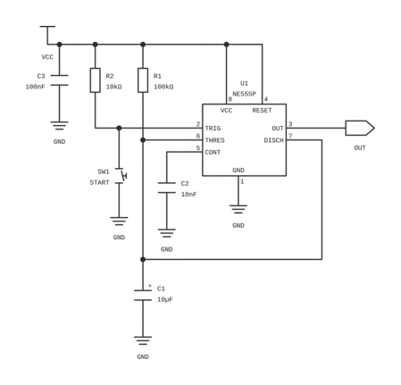
NE555 Monostable Delay Timer (One-Shot)
The one-shot circuit from the TI NE555 datasheet: press START and the output stays high for a fixed time set by one resistor and one capacitor, about 1.1 s with 100 kΩ and 10 µF.
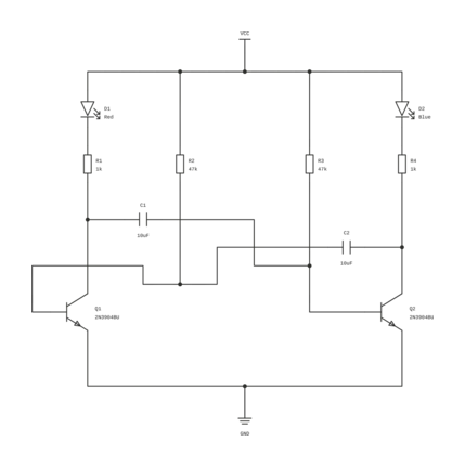

BJT Astable Multivibrator & Dual LED Flasher
Discrete two-transistor cross-coupled relaxation oscillator driving alternating LEDs without an integrated circuit.
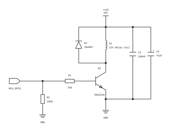
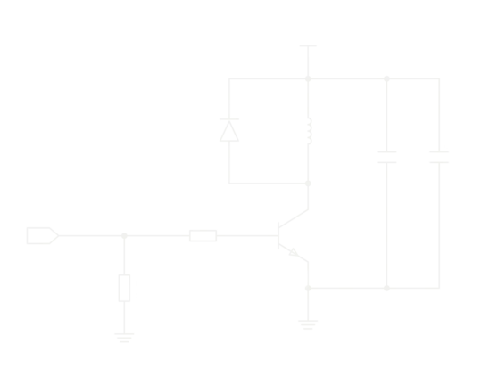
2N2222 / 2N2222A NPN BJT Relay Driver with 1N4007 Flyback Clamping Diode
Discrete NPN bipolar junction transistor low-side relay driver circuit with 1N4007 flyback suppression diode, base saturation drive, and supply decoupling for 3.3V/5V MCU control.