Analog Sensing

LM358 Inverting Operational Amplifier

Single-channel inverting amplifier using the Texas Instruments LM358 dual op-amp providing -3.6 V/V closed-loop gain from a ±12 V split supply.

Closed-Loop Voltage Gain (Av)
-3.6 V/V (-11.13 dB, 180° phase inversion)
Components
3
Formulas
3
Gotchas
4
Open in Web CAD
Verified source

Schematic workbench

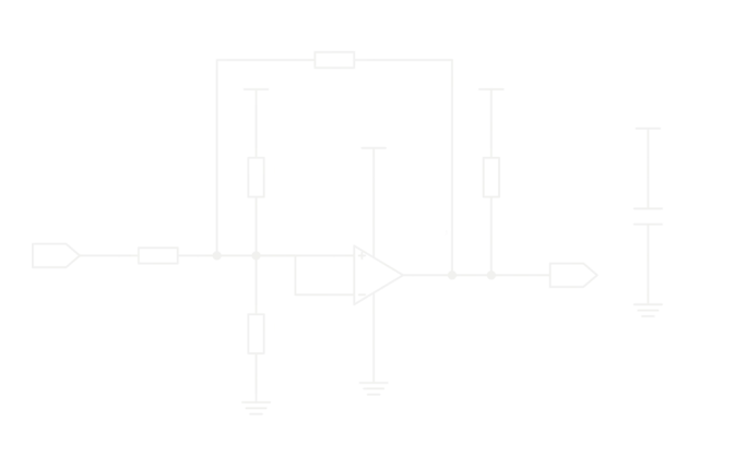
LM358 Inverting Operational AmplifierExported from CircuitBaseVINR110kΩR236kΩU1ALM358PGND+12V-12VVOUT

Circuit overview

Closed-Loop Voltage Gain (Av)
-3.6 V/V (-11.13 dB, 180° phase inversion)
Components
3
Formulas
3
Gotchas
4

Click any component in the schematic above to inspect its electrical ratings, function, and connections.

Circuit overview

This circuit implements the classic inverting amplifier from Texas Instruments LM358 datasheet SLOS068AB Figure 8-1. Operating from symmetrical ±12 V rails, it provides a closed-loop inverting gain of Av = -RF / RI = -36 kΩ / 10 kΩ = -3.6 V/V. Symmetrical dual supplies allow true bipolar signal amplification (±0.5 V input produces ∓1.8 V output) centered around ground. High open-loop gain forces the inverting terminal into a virtual ground (0 V), while negative feedback establishes high linearity, predictable frequency response up to 152 kHz, and low output impedance.

Key Technical Specifications

Closed-Loop Voltage Gain (Av)-3.6 V/V (-11.13 dB, 180° phase inversion)
Input Resistor (RI / R1)10 kΩ, 1%, 0.125 W
Feedback Resistor (RF / R2)36 kΩ, 1%, 0.125 W
Input Signal Range (VI)±0.5 V nominal (1.0 V p-p)
Output Signal Range (VO)∓1.8 V nominal (3.6 V p-p)
Power Supply Rails (V+ / V-)±12 V split supply (operates from ±1.5 V to ±16 V)
Small-Signal Bandwidth (-3 dB)≈ 152 kHz (GBW = 0.7 MHz, noise gain = 4.6)
Input Impedance (ZIN)10 kΩ (defined by R1)

Theory of Operation & Working Principle

01

Symmetrical split-rail supply

The LM358 operational amplifier is powered from symmetrical ±12 V supplies (+12 V connected to pin 8 V+, -12 V connected to pin 4 V-). Symmetrical rails ensure that the internal class-AB output stage can swing undistorted in both positive and negative directions relative to the 0 V circuit ground, enabling clean AC and bipolar DC signal amplification.
02

Virtual ground summing junction

The non-inverting input (IN+ / pin 3) connects directly to circuit ground (0 V). The op-amp internal differential input stage and high open-loop gain (A_OL ≈ 100 dB) act through the negative feedback loop to drive the differential input voltage V_ID = V+ - V- to virtually zero volts. Consequently, the inverting summing node at pin 2 is maintained at 0 V, forming an ideal virtual ground.

03

Inverting gain and feedback current balance

Because the LM358 PNP Darlington input transistors draw minimal bias current (I_B ≈ 20 nA typical), signal current arriving from input resistor R1 must flow entirely through feedback resistor R2. Applying Kirchhoff's Current Law at the inverting summing junction gives:

FORMULA & CALCULATION
IIN = (VIN - 0V) / (RI) = (0V - VOUT) / (RF)

Solving for output voltage V_OUT yields the ideal inverting amplifier transfer equation:

FORMULA & CALCULATION
VOUT = -VIN × (RF) / (RI) = -VIN × (36kΩ) / (10kΩ) = -3.6 × VIN

An input signal of ±0.5 V produces an inverted output of ∓1.8 V (180° phase inversion).

04

Input impedance and source loading

At the inverting terminal, the virtual ground sets the circuit input impedance to exactly the value of the input series resistor:

FORMULA & CALCULATION
ZIN = RI = 10kΩ

Unlike non-inverting configurations with gigohm input resistance, the inverting amplifier draws a signal current of I_IN = ±0.5 V / 10 kΩ = ±50 µA from the input source. Upstream signal generators must have low internal impedance (< 10 Ω) to avoid gain attenuation errors.

05

Dynamic bandwidth and slew rate constraints

The LM358 provides a unity-gain bandwidth product (GBW) of 0.7 MHz (700 kHz) and a slew rate of 0.3 V/µs. With a closed-loop noise gain of A_N = 1 + R_F / R_I = 1 + 3.6 = 4.6 V/V, the small-signal -3 dB bandwidth is:

FORMULA & CALCULATION
f-3dB ≈ (GBW) / (1 + (RF) / (RI)) = (700kHz) / (4.6) ≈ 152 kHz

For large output swings (3.6 V peak-to-peak), the full-power bandwidth is constrained by the 0.3 V/µs slew rate to approximately 26.5 kHz before triangular wave distortion occurs.

Design Equations & Calculations

Closed-Loop Inverting Voltage Gain

VOUT = − VIN · RFRI

Calculates the inverted output voltage based on the feedback-to-input resistance ratio.

SymbolParameterTypical value
VOUTAmplified output voltage-1.8V
VINInput signal voltage0.5V
RFFeedback resistor36kΩ
RIInput resistor10kΩ

Small-Signal Closed-Loop Bandwidth

f_{ − 3dB} = GBW1 + RFRI

Calculates the high-frequency -3 dB cutoff based on op-amp gain-bandwidth product and noise gain.

SymbolParameterTypical value
f_{ − 3dB}High-frequency -3 dB cutoff152.2kHz
GBWGain-bandwidth product700kHz
RFFeedback resistor36kΩ
RIInput resistor10kΩ

Slew Rate Limited Full-Power Bandwidth

fFPBW = SR2π · VP

Calculates the maximum frequency achievable at peak output amplitude without slew-rate distortion.

SymbolParameterTypical value
fFPBWFull-power bandwidth26.5kHz
SROp-amp slew rate0.3V/µs
VPPeak output voltage amplitude1.8V

Bill of Materials (BOM)

Every part needed to build this circuit. Select a reference designator to inspect it on the schematic.

RefDesComponentValue / ratingPackageRole in circuitReference
Dual Operational Amplifier

Texas Instruments LM358P, SLOS068AB Rev. AB; Pin 1 OUT1, Pin 2 IN1-, Pin 3 IN1+, Pin 4 GND/V-, Pin 8 V+.

LM358PPDIP-8Inverting operational amplifier (Channel A used)Dual Operational Amplifier pinout & datasheet
Input Series Resistor

10 kΩ, 1%, 0.125 W metal film resistor. Sets input impedance to 10 kΩ.

10kΩAxial / 0805Input signal scaling and impedance definition—
Feedback Resistor

36 kΩ, 1%, 0.125 W metal film resistor. Establishes closed-loop gain of -3.6 V/V.

36kΩAxial / 0805Closed-loop negative feedback—

Practical Applications & Target Domains

Precision analog signal scaling and mathematical inversion in instrumentation
Audio preamplifier inverting summing stage for active mixers
Sensor interface stage converting bipolar voltage signals for dual-rail ADCs
Foundational laboratory benchmark circuit for operational amplifier education

Critical Design Traps & Engineering Gotchas

Traps found in real builds, with the fix for each.

Critical

Class-AB Crossover Distortion Across Zero Volts

When output current reverses direction across 0 V between sourcing and sinking, the LM358 complementary output stage exhibits a deadband that creates high-frequency crossover spikes on sinusoidal signals.

Mitigation

Connect an external pull-down resistor (2 kΩ to 10 kΩ) from the output (pin 1) to the negative rail (-12 V). This keeps the top NPN transistor sourcing current continuously, forcing class-A operation and eliminating crossover distortion.

Warning

Input Bias Current DC Offset Error

The LM358 input PNP Darlington transistors have an input bias current (IB ≈ 20 nA to 100 nA) flowing out of both inputs. Tying IN+ directly to ground with 0 Ω causes an unequal DC voltage drop across RI || RF (7.83 kΩ), generating an uncompensated output offset.

Mitigation

Insert a bias compensation resistor RP = RI || RF ≈ 7.5 kΩ to 8.2 kΩ in series between IN+ (pin 3) and ground to equalize the source resistance seen by both differential inputs.

Warning

Slew Rate Limited Full-Power Bandwidth

With a 0.3 V/µs slew rate, driving large-amplitude output signals (3.6 V p-p) above 26 kHz causes slew-rate limiting, turning smooth sinusoidal waves into distorted triangular waveforms.

Mitigation

Limit large-amplitude high-frequency signals below 25 kHz. For wider bandwidth applications, substitute a pin-compatible higher-speed op-amp such as the TL072 (13 V/µs) or OPA2134 (20 V/µs).

Warning

Source Resistance Alters Closed-Loop Gain

Because circuit input impedance is defined solely by RI (10 kΩ), any internal source impedance R_source of the driving signal generator adds directly to RI, reducing effective circuit gain to -RF / (RI + R_source).

Mitigation

Drive the inverting stage from a low-impedance buffer (< 10 Ω), or calibrate RI by subtracting known source resistance so the combined sum equals 10 kΩ exactly.

Primary sources

Help keep this page accurate

Built, simulated or reviewed this circuit? Confirm it, or report a part, value or connection that is wrong.

Opens a public form on GitHub with this page already filled in; a free GitHub account is needed. How reports and confirmations work

HTML snippet

<iframe src="https://circuitbase.tech/embed/schematic/lm358-inverting-amplifier?theme=paper" width="100%" height="500" frameborder="0" loading="lazy" style="border: 1px solid #e5e7eb; border-radius: 6px; max-width: 100%;" title="LM358 Inverting Operational Amplifier — CircuitBase Interactive Schematic"></iframe>