
01
Input and volume
RV1 is a 10 kΩ potentiometer between VIN and ground. Its wiper feeds pin 3; pin 2 is grounded. Start with the volume down and keep the signal at pin 3 inside the ±0.4 V input rating.
Audio Amplifiers
TI Figure 9-9 redrawn as an editable LM386 bass-boost amplifier: a 10 kΩ and 33 nF feedback branch, volume control and an 8 Ω speaker powered from a 9 V battery.
Circuit overview
Click any component in the schematic above to inspect its electrical ratings, function, and connections.
This circuit follows Figure 9-9 of the Texas Instruments LM386 datasheet SNAS545D. A series 10 kΩ resistor and 33 nF capacitor connects pin 1 to the amplifier output at pin 5, before the output coupling capacitor. It changes the feedback with frequency, giving bass more prominence relative to the midrange and treble. Pin 8 stays open: this is not the separate gain-200 circuit. The 9 V battery and 8 Ω speaker are explicit choices within Table 9-5. The optional, unvalued BYPASS capacitor shown dashed by TI is omitted. TI recommends local supply decoupling but does not specify its value here. Application performance must be checked in the final build.
| Operating Supply Voltage | 9 V battery as drawn; 5 V to 12 V design range (TI Table 9-5) |
|---|---|
| Voltage Gain | Frequency-shaped by R2/C3; pin 8 open; no gain-200 bypass (TI Figure 9-9) |
| Load | 8 Ω speaker as drawn; design range 4 Ω to 32 Ω (TI Table 9-5) |
| Output Power | 325 mW typical, 250 mW minimum at VS = 6 V, RL = 8 Ω, THD = 10% (LM386N-1); the datasheet does not specify LM386N-1 output power at 9 V |
| Quiescent Current | 4 mA typical, 8 mA maximum at VS = 6 V, VIN = 0 (TI §6.5) |
| Input Voltage at Pin 3 | −0.4 V to +0.4 V (absolute maximum and recommended range) |
| Low-Frequency Corner | ≈ 80 Hz, calculated from C1 = 250 µF and an 8 Ω load; not measured |
| Bass Feedback Branch | R2 = 10 kΩ, C3 = 0.033 µF (33 nF), in series between pins 1 and 5 |
RV1 is a 10 kΩ potentiometer between VIN and ground. Its wiper feeds pin 3; pin 2 is grounded. Start with the volume down and keep the signal at pin 3 inside the ±0.4 V input rating.
R2 (10 kΩ) and C3 (0.033 µF) form a series path from pin 1 to pin 5. TI describes this path as paralleling the internal 15 kΩ feedback resistor. At low frequencies C3 impedes the added path; at higher frequencies it conducts more feedback, reducing gain relative to the bass region. This is a relative tone contour, not extra output-power capacity.
Pin 8 is open. TI specifies 10 kΩ as the lowest feedback resistance for good stable operation in this configuration. The separate capacitor-between-pins-1-and-8 modification for gain 200 is not fitted. The component RC benchmark is about 482 Hz; this is not the complete amplifier response or a measured bass cutoff.
Pin 5 biases to approximately half the supply, about 4.5 V at 9 V. C1 (250 µF), positive towards pin 5, blocks that DC from LS1. With an ideal 8 Ω load its calculated high-pass corner is about 80 Hz, so very low bass is still attenuated.
C2 (0.05 µF) and R1 (10 Ω) form the separate series output-to-ground network drawn by TI. Keep it distinct from the pin-1 feedback branch; R2 returns to pin 5 before C1, not to the speaker terminal after C1.
The drawing uses a 9 V battery; Table 9-5 gives 5 V to 12 V and loads from 4 Ω to 32 Ω. Pin 7 is left open, omitting the optional dashed BYPASS capacitor. Add local pin-6-to-ground decoupling and follow TI layout guidance; the reference does not assign its capacitance.
Calculated frequency at which the magnitude of C3 reactance equals R2: about 482 Hz for 10 kΩ and 33 nF. This is a component benchmark, not the full bass-response cutoff.
| Symbol | Parameter | Typical value |
|---|---|---|
| R2 | Feedback resistor | 10kΩ |
| C3 | Feedback capacitor | 33nF |
| fRC | RC benchmark (calculated) | 482Hz |
Frequency below which C1 and the speaker attenuate the signal (−3 dB), treating the speaker as a pure 8 Ω resistance.
| Symbol | Parameter | Typical value |
|---|---|---|
| RL | Speaker impedance | 8Ω |
| C1 | Output coupling capacitor | 250µF |
| fc | Corner frequency (calculated) | 80Hz |
The output biases itself to about half the supply voltage; C1 blocks this DC level from the speaker.
| Symbol | Parameter | Typical value |
|---|---|---|
| VS | Supply voltage | 9V |
| VOUT(DC) | Output bias voltage | 4.5V |
Every part needed to build this circuit. Select a reference designator to inspect it on the schematic.
| RefDes | Component | Value / rating | Package | Role in circuit | Reference |
|---|---|---|---|---|---|
| Low-Voltage Audio Power Amplifier TI LM386N-1/NOPB. LM386N-3 and LM386N-4 share the pinout but have different supply and output-power ratings. | LM386N-1 | PDIP-8 | Audio power amplifier with frequency-shaped feedback | Low-Voltage Audio Power Amplifier pinout & datasheet | |
| Rotary Potentiometer | 10kΩ | Panel / PCB mount | Volume control and input attenuator | — | |
| Aluminium Electrolytic Capacitor Datasheet value. 220 µF is the nearest common value and moves the calculated corner to about 90 Hz. Voltage rating above the supply; + towards pin 5. | 250µF | Radial | Output coupling to the speaker | — | |
| Ceramic or Film Capacitor Datasheet value; 47 nF is the nearest common value. | 0.05µF | Radial / 0805 | Output RC network | — | |
| Resistor 1/4 W | 10Ω | Axial / 0805 | Output RC network | — | |
| Loudspeaker 4 Ω to 32 Ω per TI Table 9-5. | 8Ω | Wired | Load | — | |
| 9 V Battery Any supply from 5 V to 12 V (TI Table 9-5). | 9V | PP3 / 6LR61 | Supply | — | |
| Feedback Resistor TI Figure 9-9 value. With pin 8 open, TI specifies 10 kΩ as the minimum for good stable operation. | 10kΩ | Axial / 0805 | Series bass-feedback branch | — | |
| Feedback Capacitor 33 nF, the 0.033 µF of TI Figure 9-9. Non-polarized. | 0.033µF | Radial / 0805 | Frequency shaping in series with R2 | — |
Traps found in real builds, with the fix for each.
The absolute maximum input voltage is ±0.4 V. A headphone or line-level signal can be larger; fed straight to pin 3 it can exceed that rating, and the output clips well before the input reaches it.
Keep RV1 between the source and pin 3 as drawn and start with the volume turned down; keep the signal at pin 3 within ±0.4 V.
Figure 9-9 draws no capacitor on the supply, but TI recommends one close to pin 6. Without it, long battery leads and supply ripple reach the output as hum or instability.
Add a capacitor from pin 6 to GND right next to the IC (the datasheet does not give a value) and keep the speaker leads short (TI §10, §11.1).
Pin 5 sits at about half the supply, so C1 has a steady DC voltage across it. An electrolytic fitted the wrong way round is reverse-biased.
Fit C1 with its positive terminal towards pin 5 and the negative terminal towards the speaker, and use a voltage rating above the supply voltage.
A smaller R2 with pin 8 open can reduce the closed-loop gain below the range for which the LM386 is compensated. TI gives 10 kΩ as the minimum for good stable operation in this arrangement.
Keep R2 at 10 kΩ or above with pin 8 open, as in Figure 9-9. Connect the RC branch to pin 5 before C1. Do not combine it with a gain-200 modification without redesign and validation.
Built, simulated or reviewed this circuit? Confirm it, or report a part, value or connection that is wrong.
Opens a public form on GitHub with this page already filled in; a free GitHub account is needed. How reports and confirmations work
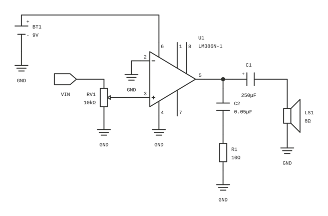
The minimum-parts speaker amplifier from the TI LM386 datasheet: a volume potentiometer, the LM386 at its internal gain of 20, an output capacitor and an RC network driving an 8 Ω speaker from a 9 V battery.
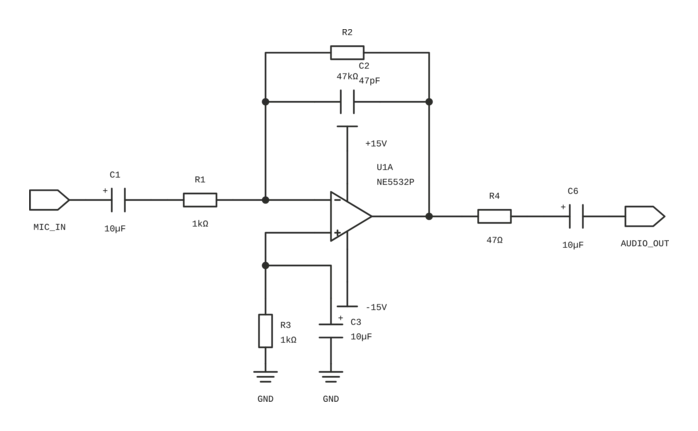
Single-channel ultra-low-noise inverting audio preamplifier based on the Texas Instruments NE5532 op-amp, featuring +33.4 dB closed-loop gain, input DC blocking, and high-frequency phase compensation.
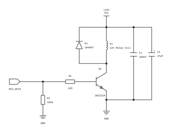
Discrete NPN bipolar junction transistor low-side relay driver circuit with 1N4007 flyback suppression diode, base saturation drive, and supply decoupling for 3.3V/5V MCU control.