
01
Supply and input bypass
A nominal 10 V unregulated or pre-regulated DC supply is connected to input port P1. Ceramic capacitor C1 (100 nF, 50 V) provides high-frequency decoupling directly at the input to suppress rail noise and ripple.
Power & Supplies
Texas Instruments TL431 programmable precision shunt voltage reference circuit producing 5.0 V nominal from a 10 V rail with a 470 Ω bias resistor and 10 kΩ / 10 kΩ divider.
Circuit overview
Click any component in the schematic above to inspect its electrical ratings, function, and connections.
This circuit implements the classic programmable shunt regulator from Texas Instruments datasheet SLVS543S Figure 9-3. The TL431 acts as a precision shunt reference maintaining 2.495 V at its REF terminal via an internal bandgap and operational error amplifier driving an open-collector NPN Darlington transistor. A precision resistive divider (R1 and R2) sets the nominal output voltage to 5.01 V (approx. 5.0 V). Series resistor R3 (470 Ω) drops the 10 V input supply, providing approximately 10.4 mA of cathode bias current to guarantee operation well above the 1.0 mA minimum cathode current requirement (Imin). Input capacitor C1 (100 nF) bypasses supply transients. Operating stability requires respecting the capacitive load boundary (TI Fig. 8-16), avoiding direct capacitive loading in the forbidden 10 nF to 3 µF range.
| Input Operating Voltage | 10 V nominal (operates from 8 V to 15 V with appropriate R3 sizing) |
|---|---|
| Regulated Output Voltage | ≈ 5.01 V nominal calculation (2.495 V * 2 + 2 µA * 10 kΩ) |
| Reference Voltage (Vref) | 2.495 V nominal; 2.440 V to 2.550 V standard grade (TI SLVS543S §6.5) |
| Cathode Bias Current (IK) | ≈ 10.4 mA nominal at no load (safe operating range: 1.0 mA to 100 mA) |
| Feedback Divider Current | ≈ 250 µA (Vref / R2 = 2.495 V / 10 kΩ) |
| Series Bias Resistor (R3) | 470 Ω, 1%, 0.25 W (nominal dissipation ≈ 53 mW) |
| Dynamic Impedance (|ZKA|) | 0.2 Ω typical, 0.5 Ω maximum (f < 1 kHz) |
A nominal 10 V unregulated or pre-regulated DC supply is connected to input port P1. Ceramic capacitor C1 (100 nF, 50 V) provides high-frequency decoupling directly at the input to suppress rail noise and ripple.
Resistor R3 (470 Ω, 1%, 1/4 W) sits between the 10 V input and the 5.0 V regulated cathode node. With a 5.0 V drop across R3, the total current supplied is I_RS = (10 V - 5.0 V) / 470 Ω ≈ 10.64 mA. This current splits between the feedback divider (≈ 0.25 mA), the TL431 cathode (≈ 10.39 mA), and any external load connected to P2.
The internal reference amplifier compares the voltage at pin 1 (REF) against the internal 2.495 V temperature-compensated bandgap reference. The output voltage is programmed by R1 and R2 according to V_O = V_ref * (1 + R1/R2) + I_ref * R1. With R1 = 10 kΩ, R2 = 10 kΩ, and I_ref ≈ 2 µA, the nominal output is 2.495 V * 2 + 20 mV = 5.01 V ≈ 5.0 V.
If V_OUT rises slightly, V_REF exceeds 2.495 V, causing the internal amplifier to increase base drive to the output NPN transistor. The transistor shunts more cathode current to GND through pin 2 (ANODE), increasing the voltage drop across series resistor R3 and pulling V_OUT back down to the programmed setpoint. Conversely, if V_OUT drops, the transistor conducts less, restoring regulation.
The internal error amplifier has high open-loop gain and compensation designed for stable shunt regulation. However, as documented in TI SLVS543S Figure 8-16, connecting capacitive loads directly between Cathode and Anode within the range of 10 nF to 3 µF introduces an unfavorable pole-zero phase shift that degrades phase margin and causes oscillation. The circuit is fully stable with no load capacitor or with C_L ≥ 10 µF (with typical ESR damping).
Calculates the regulated output voltage based on the reference divider and input bias current.
| Symbol | Parameter | Typical value |
|---|---|---|
| Vref | Internal reference voltage | 2.495V |
| R1 | Upper divider resistor | 10000Ω |
| R2 | Lower divider resistor | 10000Ω |
| Iref | Reference input current | 2e-6A |
Total current delivered through the series ballast resistor to the shunt regulator and load.
| Symbol | Parameter | Typical value |
|---|---|---|
| VI | Input supply voltage | 10V |
| VO | Regulated output voltage | 5.01V |
| R3 | Series bias resistor | 470Ω |
Current flowing through the TL431 cathode. Must remain >= 1.0 mA under all conditions.
| Symbol | Parameter | Typical value |
|---|---|---|
| IRS | Ballast resistor current | 10.64mA |
| Vref | Reference voltage | 2.495V |
| R2 | Lower divider resistor | 10kΩ |
| IL | External load current | 0mA |
Every part needed to build this circuit. Select a reference designator to inspect it on the schematic.
| RefDes | Component | Value / rating | Package | Role in circuit | Reference |
|---|---|---|---|---|---|
| Precision Programmable Shunt Regulator Texas Instruments TL431LP, SLVS543S Rev. S; Pin 1 REF, Pin 2 ANODE, Pin 3 CATHODE. | TL431LP | TO-92 | Shunt voltage regulator and error amplifier | Precision Programmable Shunt Regulator pinout & datasheet | |
| Series Bias Resistor Selected 470 Ω, 1%, 0.25 W. Dissipates ≈ 53 mW nominal at 10 V input. | 470Ω | Axial / 0805 | Limits input current and establishes cathode bias | — | |
| Upper Divider Resistor 10 kΩ, 0.1% or 1%, 0.125 W. Sets nominal output ratio with R2. | 10kΩ | Axial / 0805 | Upper leg of output voltage setting divider | — | |
| Lower Divider Resistor 10 kΩ, 0.1% or 1%, 0.125 W. Senses Vref = 2.495 V to GND. | 10kΩ | Axial / 0805 | Lower leg of output voltage setting divider | — | |
| Input Supply Bypass Capacitor 100 nF, 50 V ceramic X7R. Placed near P1 and R3 input node. | 100nF | Radial / 0805 | Input supply transient decoupling | — |
Traps found in real builds, with the fix for each.
Connecting bypass capacitors directly across Cathode and Anode between 10 nF and 3 µF causes sustained high-frequency parasitic oscillation due to loss of phase margin (TI SLVS543S Figure 8-16).
Leave the output unbypassed (pure resistive divider) or use a bulk capacitor CL ≥ 10 µF with normal electrolytic ESR (0.5 to 2 Ω). If a ceramic capacitor is mandatory, add a 1 to 3 Ω series damping resistor.
The internal bandgap and comparator circuits require a minimum cathode current Imin = 1.0 mA. If load current IL exceeds IRS - 1.0 mA, IK drops below 1.0 mA and regulation is completely lost.
Ensure R3 is sized so that under maximum load current and minimum input voltage, IRS - IL >= 1.5 mA. For loads exceeding 10 mA, use an external PNP pass transistor.
Using high-value divider resistors (e.g. R1, R2 > 100 kΩ) to reduce divider current amplifies the error caused by the reference input current Iref (up to 4 µA) and its temperature drift.
Select R1 and R2 such that divider current is at least 100 times Iref (IDIV >= 200 µA). The chosen 10 kΩ resistors draw 250 µA, keeping Iref offset to just 20 mV.
If the output is accidentally shorted to ground, the full 10 V supply drops across R3, increasing dissipation to (10 V)^2 / 470 Ω = 213 mW.
Specify R3 with at least a 0.25 W (1/4 W) power rating so it tolerates continuous output short circuits without thermal damage.
Built, simulated or reviewed this circuit? Confirm it, or report a part, value or connection that is wrong.
Opens a public form on GitHub with this page already filled in; a free GitHub account is needed. How reports and confirmations work
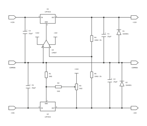

The ±15 V, 1 A tracking regulator from the TI LM79xx datasheet: an LM7915 trimmed to exactly −15 V and an LM7815 whose ground pin is driven by an LM307 op-amp, so the positive rail mirrors the negative one.
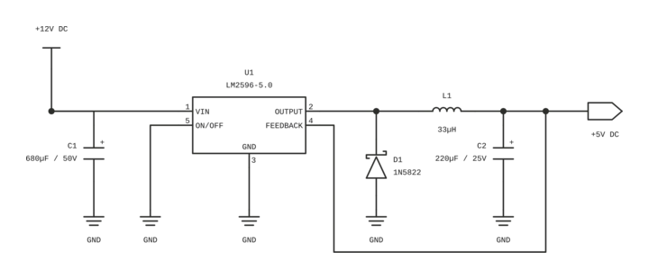
High-efficiency 150-kHz step-down switching regulator delivering a regulated 5V output at up to 3A continuous load from a 7V–40V DC supply with minimal external components.
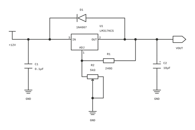
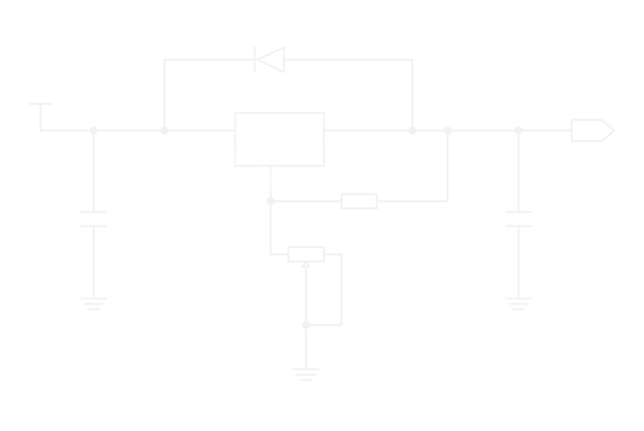
Adjustable DC voltage reference circuit using TI LM317KCS and nominal 12V input. Calculated setpoints up to 9V respect the recommended 3V headroom; usable current requires a load and thermal budget.