01
Reference and minimum load
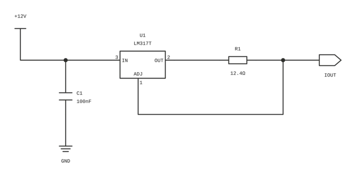
U1 regulates the OUT-to-ADJ differential to nominal VREF=1.25V. TI §6.6 specifies 1.20–1.30V under its stated differential, current and power conditions: 3V≤VIN−VOUT≤40V, 10mA≤IOUT≤1.5A and PD≤20W. These IC conditions do not establish a tested rating for this assembly.
R1=240Ω carries a calculated nominal current I1=1.25V/240Ω≈5.21mA. TI lists minimum load as 3.5mA typical and 10mA maximum at VIN−VOUT=40V across its operating temperature range. The divider therefore relies on typical behavior without an external load. Even a nominal 120Ω resistor with +1% tolerance gives only 1.20V/121.2Ω≈9.90mA at the minimum reference voltage. Check the complete tolerance and load budget rather than assuming worst-case regulation.