
01
Supply and bypass
Apply the selected 12 V supply to IN and connect the load return to GND. C1 is a 100 nF input bypass following ST §6; keep it near the IC. Figure 9 itself has no capacitor.
Power & Supplies
ST LM317T current regulator with a 12.4 Ω sense resistor for about 100 mA, 12 V nominal input and an input bypass capacitor. The external load connects between IOUT and GND.
Circuit overview
Click any component in the schematic above to inspect its electrical ratings, function, and connections.
The circuit redraws ST DS0433 Figure 9: R1 sits between OUT and the load, and ADJ senses the load side of R1. The regulator maintains about 1.25 V across R1. Its current and the small ADJ current flow into the load. The selected 12.4 Ω, 1% resistor gives about 100.9 mA nominal, not a guaranteed 1% current. The 12 V source, 0.5 W resistor and 100 nF input bypass are explicit design choices. The load is external. Regulation needs voltage headroom and adequate cooling; this is neither a complete battery charger nor a guaranteed precision LED driver.
| Input Operating Voltage | 12 V selected; load voltage and regulator headroom must fit within it |
|---|---|
| Current Setpoint | ≈ 100.9 mA calculated: 1.25 V / 12.4 Ω + 50 µA |
| Reference Voltage | 1.20 V to 1.30 V; 1.25 V nominal (ST Table 4 conditions) |
| Adjustment Current | 50 µA typical, 100 µA maximum (ST Table 4) |
| Sense Resistor | 12.4 Ω, 1%, 0.5 W selected; ≈ 0.126 W nominal dissipation |
| Load Voltage Budget | 7.75 V nominal calculation at 12 V with a selected 3 V regulator reserve; not a guaranteed rating |
| Operating Junction Temperature | 0 °C to 125 °C for ST LM317 (ST Table 1) |
Apply the selected 12 V supply to IN and connect the load return to GND. C1 is a 100 nF input bypass following ST §6; keep it near the IC. Figure 9 itself has no capacitor.
OUT feeds R1, then IOUT. ADJ connects to IOUT, not GND. This closes the feedback around R1 and holds about 1.25 V across it. The tab is OUT, upstream of R1.
With R1 = 12.4 Ω and nominal IADJ = 50 µA, the calculated load current is about 100.9 mA. ST Table 4 gives VREF = 1.20 V to 1.30 V and IADJ up to 100 µA under its stated conditions. With a 1% resistor and IADJ treated as 0 to 100 µA, the calculated envelope is about 95.8 mA to 106.0 mA. This excludes resistor temperature drift and self-heating and is not a measured result.
The load does not see a fixed output voltage. For the selected 12 V input, a nominal 1.25 V sense drop and an engineering reserve of 3 V across the regulator leave 7.75 V for the load. This is a design budget, not a guaranteed compliance voltage or exact dropout threshold. Account for supply ripple and temperature. An open load stops regulation and may let IOUT rise towards the supply.
R1 dissipates about 0.126 W nominal; its selected 0.5 W rating still needs ambient derating. A shorted load can leave about 1.08 W in the LM317T at the nominal setpoint. Check the thermal path for the actual mounting and keep the operating junction within 0 °C to 125 °C. Internal thermal and current protection do not establish safe normal operation.
About 100.9 mA for the selected resistor and nominal ST reference and ADJ current.
| Symbol | Parameter | Typical value |
|---|---|---|
| VREF | Reference voltage | 1.25V |
| R1 | Sense resistance | 12.4Ω |
| IADJ | Adjustment current | 50µA |
About 0.126 W nominal; the selected 0.5 W resistor still requires ambient-temperature derating.
| Symbol | Parameter | Typical value |
|---|---|---|
| VREF | Reference voltage | 1.25V |
| R1 | Sense resistance | 12.4Ω |
| PR1 | Calculated resistor dissipation | 0.126W |
Nominal engineering budget of 7.75 V. The selected 3 V reserve is not an exact ST dropout specification.
| Symbol | Parameter | Typical value |
|---|---|---|
| VIN | Selected input voltage | 12V |
| VREF | Nominal sense drop | 1.25V |
| VRESERVE | Selected regulator reserve | 3V |
Every part needed to build this circuit. Select a reference designator to inspect it on the schematic.
| RefDes | Component | Value / rating | Package | Role in circuit | Reference |
|---|---|---|---|---|---|
| Adjustable Linear Regulator STMicroelectronics LM317T, DS0433 Rev 22; not the TI LM317KCS used on the separate voltage-regulator page. | LM317T | TO-220 | Maintains the voltage across R1 | Adjustable Linear Regulator pinout & datasheet | |
| Current Sense Resistor Selected 1%, 0.5 W minimum nominal rating; check temperature coefficient and ambient derating. This value is a CircuitBase example, not a value printed in ST Figure 9. | 12.4Ω | Axial | Programs about 100 mA | — | |
| Input Bypass Capacitor 100 nF following ST §6. Select a voltage rating above the maximum actual supply; capacitor and load are not drawn in Figure 9. | 100nF | Radial / 0805 | Local supply bypass | — |
Traps found in real builds, with the fix for each.
Grounding ADJ turns this topology into a voltage regulator. Taking the load directly from OUT bypasses R1 and its programmed current limit.
Connect OUT pin 2 to R1, the other end of R1 to IOUT, and ADJ pin 1 to IOUT. Connect the external load from IOUT to GND.
A high load voltage leaves too little voltage across R1 and the regulator; the current then falls below the calculated setpoint.
Budget VIN for the load voltage, sense drop and regulator reserve. The selected 12 V example leaves 7.75 V nominal with a 3 V reserve; evaluate ripple and temperature.
A 1% resistor does not make a 1% current source. Reference spread, ADJ current, temperature drift and self-heating also contribute.
Use the 95.8 mA to 106.0 mA calculated envelope only with its stated assumptions. Check resistor derating and measure the assembled current before connecting a sensitive load.
A shorted load maximizes regulator dissipation in this example; an open load does not hold IOUT at a safe low voltage. The metal tab is OUT, not GND.
Evaluate about 1.08 W nominal short-load dissipation and provide a suitable thermal path. Switch off before changing loads, insulate the tab where needed, and add load-specific protection or charging control.
Built, simulated or reviewed this circuit? Confirm it, or report a part, value or connection that is wrong.
Opens a public form on GitHub with this page already filled in; a free GitHub account is needed. How reports and confirmations work
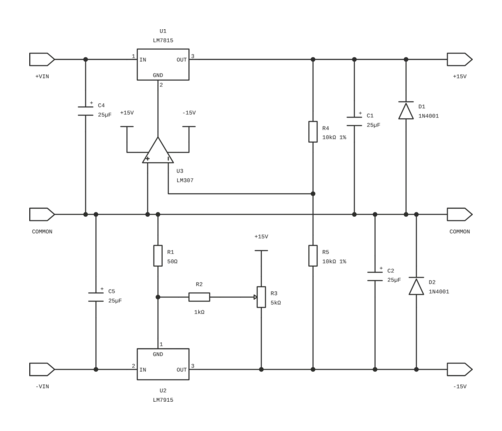
The ±15 V, 1 A tracking regulator from the TI LM79xx datasheet: an LM7915 trimmed to exactly −15 V and an LM7815 whose ground pin is driven by an LM307 op-amp, so the positive rail mirrors the negative one.
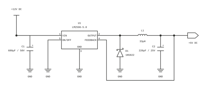
High-efficiency 150-kHz step-down switching regulator delivering a regulated 5V output at up to 3A continuous load from a 7V–40V DC supply with minimal external components.
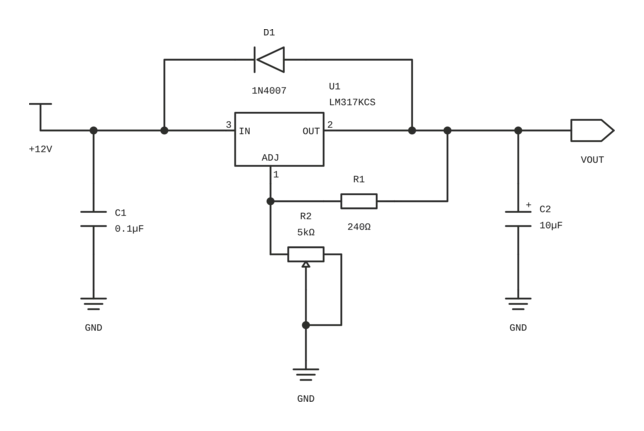
Adjustable DC voltage reference circuit using TI LM317KCS and nominal 12V input. Calculated setpoints up to 9V respect the recommended 3V headroom; usable current requires a load and thermal budget.