LM7805 5V Linear Regulator with Decoupling (L7805CV)
A nominal 9V-to-5V supply using ST L7805CV, input/output bypass capacitors, a discharge-path diode and an LED indicator. Includes conditional ratings and thermal calculations.
Illustrated supply
9V DC nominal input; 5V nominal output; no bench measurement
9V DC nominal input; 5V nominal output; no bench measurement
Components
8
Formulas
3
Gotchas
4
Click any component in the schematic above to inspect its electrical ratings, function, and connections.
Circuit overview
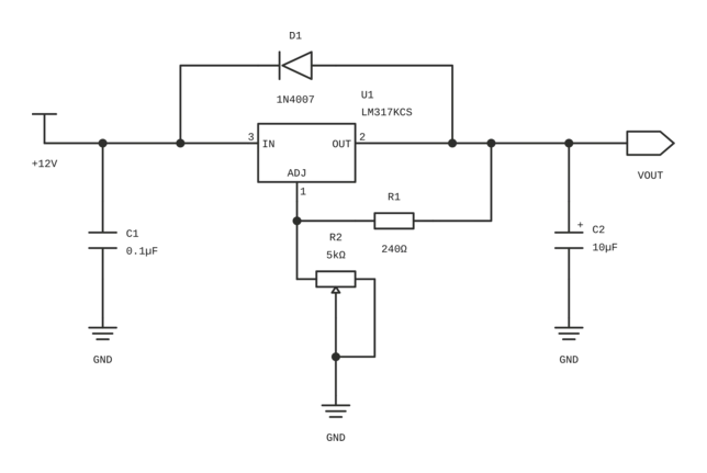
This circuit uses STMicroelectronics L7805CV in TO-220. Its values come from ST L78 datasheet DS0422 Rev 38 (February 2025), not from the onsemi or TI versions of the 7805 family. The linked LM7805 component page is a family reference; use the ST limits stated here for U1. The drawing adapts the fixed-output application in Figure 8 (page 22) with additional bulk storage, an LED branch and an optional output-to-input discharge path.
The illustrated input is 9V DC and the output is nominally 5V. Table 10 (page 13) specifies 4.75–5.25V over VIN=7–18V, IOUT=5mA–1A and TJ=0–125°C; the narrower 4.8–5.2V row applies at TJ=25°C under the table conditions. These are IC specifications, not a tested continuous-current rating for this assembly. Available load current depends on temperature, input voltage, layout and cooling.
C2=330nF and C3=100nF follow the input/output bypass values in Figure 8. ST states that the input bypass is required when the regulator is far from the supply filter; the output capacitor improves transient response and is not required for stability. C1=10µF and C4=100µF provide additional local storage. Keep bypass connections short and verify the selected capacitors under bias and temperature.
D1 is a Vishay 1N4007 in DO-41, connected with anode at VOUT and cathode at VIN. This is an additional discharge path, not reverse-input-polarity protection. ST Figure 27 (page 29) discusses destructive reverse discharge for high-capacitance loads above 6V; it does not establish that this 5V/100µF circuit always needs D1 or otherwise fails. Check discharge energy and the input supply's ability to accept returned current. D1 ratings are taken separately from Vishay document 88503: https://www.vishay.com/docs/88503/1n4001.pdf .
R1=330Ω limits current through a generic green LED. The LED indicates that voltage is present; it does not verify output accuracy or power-good timing. No physical bench test, automotive transient qualification or complete assembly current rating is claimed.
Key Technical Specifications
Illustrated supply
9V DC nominal input; 5V nominal output; no bench measurement
Regulated Output Voltage
4.75–5.25V at VIN=7–18V, IOUT=5mA–1A, TJ=0–125°C (ST Table 10)
Assembly load current
Not established; calculate temperature and cooling for the intended load
Dropout voltage
2V typical at IOUT=1A, TJ=25°C (ST Table 10)
Ground current
8mA maximum at TJ=25°C under ST Table 10 conditions
U1 junction operating range
0–125°C for L7805C (ST Table 1)
U1 absolute input stress limit
35V (ST Table 1); not an assembly operating rating
Theory of Operation & Working Principle
01
Input bypass and regulation
P_VIN supplies nominal 9V DC to U1Pin 1. C1 and C2 connect to the common ground net. U1 regulates Pin 3 relative to Pin 2 (GND); the TO-220 tab is also ground. The regulator dissipates the input-output voltage difference as heat.
02
Output storage and indication
C3 and C4 connect from VOUT to GND. R1 and LED1 form a separate series branch. Include LED current in the total regulator output current. Table 10 specifies a 5mA minimum load for regulation; do not assume a generic LED branch guarantees this minimum under every condition.
03
Dropout and source conditions
The 2V dropout figure is typical at IOUT=1A and TJ=25°C, not a universal guaranteed overhead. Use the qualified Table 10 voltage/load/temperature conditions and allow for supply ripple and wiring losses. A nominal 6V source is outside that output-voltage specification.
04
Heat calculation
Estimate regulator dissipation with total output current, including the indicator:
FORMULA & CALCULATION
PD ≈ (VIN-VOUT) IOUT+VIN IG
05
Output-to-input discharge
D1 normally blocks because VIN exceeds VOUT. If VIN collapses below the charged output, D1 can conduct back toward the input. It does not limit the capacitor's surge current by itself. Input faults, discharge path impedance and diode pulse capability must be evaluated for the intended supply.
Design Equations & Calculations
Regulator dissipation estimate
PD ≈ (VIN − VOUT) · IOUT + VIN · IG
Illustrative DC estimate; total IOUT includes the LED branch. IG=8mA is the ST maximum at TJ=25°C, used as an assumption here.
Symbol
Parameter
Typical value
VIN
Illustrative input voltage
9V
VOUT
Nominal output voltage
5V
IOUT
Illustrative total output current
0.1A
IG
Assumed ground current
0.008A
Junction temperature estimate
TJ ≈ TA + PD · θJA
First-order estimate for the assumed mounting; 48.6°C is calculated, not measured. Check actual board and cooling.
Symbol
Parameter
Typical value
TA
Assumed ambient temperature
25°C
PD
Calculated dissipation
0.472W
θJA
ST TO-220 junction-to-ambient thermal resistance
50°C/W
Indicator current estimate
ILED ≈ VOUT − VFR1
VF depends on the selected LED and operating current; no exact LED current is asserted.
Symbol
Parameter
Typical value
VOUT
Nominal output voltage
5V
VF
Selected LED forward voltage
—V
R1
Series resistance
330Ω
Bill of Materials (BOM)
Every part needed to build this circuit. Select a reference designator to inspect it on the schematic.
RefDes
Component
Value / rating
Package
Role in circuit
Reference
STMicroelectronics L7805CV
ST DS0422 Rev 38; Pins 1 IN, 2 GND, 3 OUT; tab GND. Family page uses a different reference manufacturer.
Vishay 88503: IF(AV)=1A at TA=75°C, 9.5mm lead length; IFSM=30A at TA=25°C, non-repetitive 8.3ms half-sine superimposed on rated load. Check actual discharge.
1N4007
DO-41
Additional output-to-input discharge path
—
Generic input bulk capacitor
Observe polarity; generic part, select footprint and ripple-current rating for the assembly.
10µF / 25V
Radial electrolytic
Local input charge storage
—
Generic ceramic input bypass
X7R; keep connections to Pin 1 and GND short. Figure 8 value.
330nF / 50V
0805
Input bypass
—
Generic ceramic output bypass
X7R; Figure 8 says output capacitor improves transient response, not required for stability.
100nF / 25V
0805
Output transient bypass
—
Generic output bulk capacitor
Observe polarity; additional adaptation, evaluate discharge and load transients.
100µF / 16V
Radial electrolytic
Local output charge storage
—
Generic LED series resistor
Select tolerance and verify dissipation with the chosen LED; no exact current is claimed.
330Ω / 0.25W
Axial
LED current limiting
—
Generic green indicator LED
Select a specific LED with suitable current and forward-voltage ratings; not a power-good monitor.
Green LED
Through-hole
Output-voltage indication
—
Practical Applications & Target Domains
✓Local 5V DC supply for logic circuits within the calculated load budget
✓Linear post-regulation where input headroom and heat dissipation have been checked
✓Educational study of bypassing, dropout and regulator thermal design
Critical Design Traps & Engineering Gotchas
Traps found in real builds, with the fix for each.
Warning
Thermal budget limits usable current
The IC family current headline does not establish continuous current for this assembly. Higher input voltage increases dissipation.
Mitigation
Calculate PD and TJ using the actual ambient, mounting and heatsink. Keep L7805C within its 0–125°C operating junction range; do not rely on thermal shutdown for normal operation.
Warning
Typical dropout is not guaranteed headroom
Adding a typical 2V dropout to 5V does not guarantee regulation at all loads and temperatures. Supply ripple can reduce instantaneous input voltage.
Mitigation
Use ST Table 10 conditions and check the lowest input voltage at the actual load. The illustrated 9V input is a nominal design point, not a measured operating range.
Warning
A discharge diode is not input protection
D1 returns output charge toward VIN. It does not protect against a reversed supply, clamp input surges or guarantee safe discharge into every source.
Mitigation
Check D1 polarity (anode VOUT, cathode VIN), discharge energy and source reverse-current tolerance. ST Figure 27 explicitly concerns high-capacitance outputs above 6V; D1 is an additional adaptation here.
Note
Indicator and minimum load
A lit LED does not prove a regulated 5V output. A generic LED forward voltage does not establish a guaranteed load current.
Mitigation
Verify at least the specified 5mA load when using the Table 10 regulation limits. Select LED1 and R1 for their current/power ratings and include indicator current in IOUT.
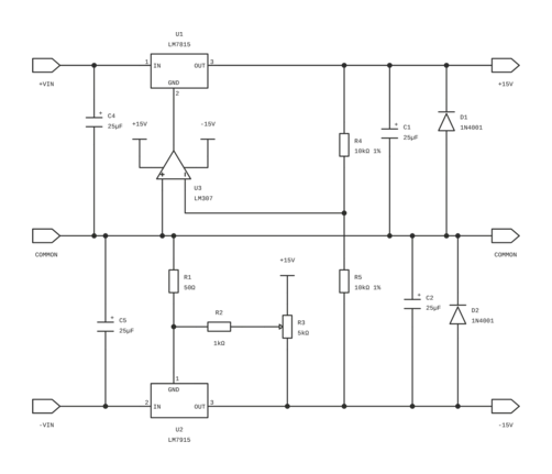
The ±15 V, 1 A tracking regulator from the TI LM79xx datasheet: an LM7915 trimmed to exactly −15 V and an LM7815 whose ground pin is driven by an LM307 op-amp, so the positive rail mirrors the negative one.
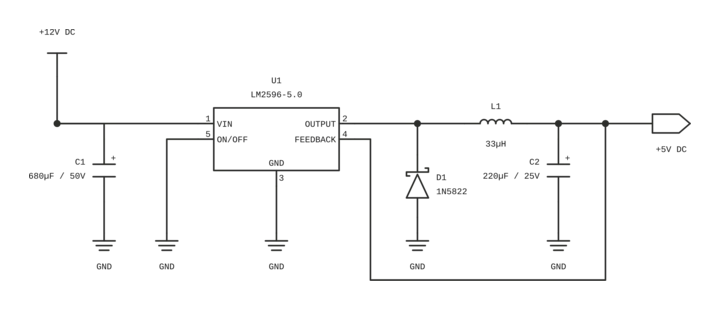
High-efficiency 150-kHz step-down switching regulator delivering a regulated 5V output at up to 3A continuous load from a 7V–40V DC supply with minimal external components.
Adjustable DC voltage reference circuit using TI LM317KCS and nominal 12V input. Calculated setpoints up to 9V respect the recommended 3V headroom; usable current requires a load and thermal budget.